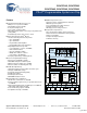
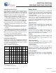
CY8C27143, CY8C27243 CY8C27443, CY8C27543, CY8C27643 PSoC® Programmable System-on-Chip Features ■ ■ ■ ■ ■ Powerful Harvard Architecture Processor ❐ M8C processor speeds to 24 MHz ❐ 8x8 multiply, 32-bit accumulate ❐ Low power at high speed ❐ 3.0 to 5.25V operating voltage ❐ Operating voltages down to 1.
CY8C27143, CY8C27243 CY8C27443, CY8C27543, CY8C27643 Contents Features ...............................................................................1 Logic Block Diagram ..........................................................1 Contents ..............................................................................2 PSoC Functional Overview ................................................3 PSoC Core ....................................................................3 Digital System ....................
CY8C27143, CY8C27243 CY8C27443, CY8C27543, CY8C27643 PSoC Functional Overview The PSoC family consists of many Programmable System-on-Chip Controller devices. These devices are designed to replace multiple traditional MCU-based system components with one, low cost single-chip programmable device. PSoC devices include configurable blocks of analog and digital logic, as well as programmable interconnects.
CY8C27143, CY8C27243 CY8C27443, CY8C27543, CY8C27643 The Analog System is composed of 12 configurable blocks, each comprised of an opamp circuit allowing the creation of complex analog signal flows. Analog peripherals are very flexible and can be customized to support specific application requirements. Some of the more common PSoC analog functions (most available as user modules) are listed below.
CY8C27143, CY8C27243 CY8C27443, CY8C27543, CY8C27643 Getting Started Additional System Resources System Resources, some of which have been previously listed, provide additional capability useful to complete systems. Additional resources include a multiplier, decimator, switch mode pump, low voltage detection, and power on reset. Statements describing the merits of each system resource are below. ■ Digital clock dividers provide three customizable clock frequencies for use in applications.
CY8C27143, CY8C27243 CY8C27443, CY8C27543, CY8C27643 Development Tools PSoC Designer is a Microsoft® Windows-based, integrated development environment for the Programmable System-on-Chip (PSoC) devices. The PSoC Designer IDE runs on Windows XP or Windows Vista. This system provides design database management by project, an integrated debugger with In-Circuit Emulator, in-system programming support, and built in support for third party assemblers and C compilers.
CY8C27143, CY8C27243 CY8C27443, CY8C27543, CY8C27643 Designing with PSoC Designer The development process for the PSoC device differs from that of a traditional fixed function microprocessor. The configurable analog and digital hardware blocks give the PSoC architecture a unique flexibility that pays dividends in managing specification change during development and by lowering inventory costs.
CY8C27143, CY8C27243 CY8C27443, CY8C27543, CY8C27643 Document Conventions Units of Measure Acronyms Used This table lists the acronyms used in this data sheet. A units of measure table is located in the section Electrical Specifications on page 19. Table 13 on page 19 lists all the abbreviations used to measure the PSoC devices. Table 2.
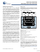
CY8C27143, CY8C27243 CY8C27443, CY8C27543, CY8C27643 Pinouts The CY8C27x43 PSoC device is available in a variety of packages which are listed and illustrated in the following tables. Every port pin (labeled with a “P”) is capable of Digital I/O. However, Vss, Vdd, SMP, and XRES are not capable of Digital I/O. 8-Pin Part Pinout Table 3. Pin Definitions - 8-Pin PDIP Type Pin No. Digital Analog Pin Name 1 I/O I/O P0[5] Analog column mux input and column output.
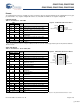
CY8C27143, CY8C27243 CY8C27443, CY8C27543, CY8C27643 28-Pin Part Pinout Table 5. Pin Definitions - 28-Pin PDIP, SSOP, SOIC 1 I/O I P0[7] Analog column mux input. 2 I/O I/O P0[5] Analog column mux input and column output. 3 I/O I/O P0[3] Analog column mux input and column output. 4 I/O I P0[1] Analog column mux input. 5 I/O 6 I/O 7 I/O I P2[3] 8 I/O I P2[1] Direct switched capacitor block input. SMP Switch Mode Pump (SMP) connection to external components required.
CY8C27143, CY8C27243 CY8C27443, CY8C27543, CY8C27643 44-Pin Part Pinout Table 6. Pin Definitions - 44-Pin TQFP Pin No.
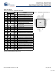
CY8C27143, CY8C27243 CY8C27443, CY8C27543, CY8C27643 48-Pin Part Pinout Table 7. 48-Pin Part Pinout (SSOP) Pin No. Type Digital Analog Pin Name Description 1 I/O I P0[7] Analog column mux input. 2 I/O I/O P0[5] Analog column mux input and column output. 3 I/O I/O P0[3] Analog column mux input and column output. 4 I/O I P0[1] Analog column mux input. 5 I/O 6 I/O 7 I/O I P2[3] Direct switched capacitor block input. 8 I/O I P2[1] Direct switched capacitor block input.
CY8C27143, CY8C27243 CY8C27443, CY8C27543, CY8C27643 Table 8. 48-Pin Part Pinout (QFN)* Description I/O I P2[3] Direct switched capacitor block input. 2 I/O I P2[1] Direct switched capacitor block input. 3 I/O P4[7] 4 I/O P4[5] 5 I/O P4[3] 6 I/O P4[1] Power SMP Switch Mode Pump (SMP) connection to external components required. 8 I/O P3[7] 9 I/O P3[5] 10 I/O P3[3] 11 I/O P3[1] 12 I/O P5[3] 13 I/O P5[1] 14 I/O P1[7] I2C Serial Clock (SCL).
CY8C27143, CY8C27243 CY8C27443, CY8C27543, CY8C27643 56-Pin Part Pinout The 56-pin SSOP part is for the CY8C27002 On-Chip Debug (OCD) PSoC device. Note This part is only used for in-circuit debugging. It is NOT available for production. Table 9. 56-Pin Part Pinout (SSOP) Pin No. Type Digital Analog 1 Pin Name Description NC No connection. 2 I/O I P0[7] Analog column mux input. 3 I/O I P0[5] Analog column mux input and column output.
CY8C27143, CY8C27243 CY8C27443, CY8C27543, CY8C27643 Table 9. 56-Pin Part Pinout (SSOP) 42 OCD HCLK OCD high-speed clock output. 43 OCD CCLK OCD CPU clock output. 44 I/O P4[0] 45 I/O P4[2] 46 I/O P4[4] 47 I/O 48 I/O I P2[0] Direct switched capacitor block input. 49 I/O I P2[2] Direct switched capacitor block input. 50 I/O P2[4] External Analog Ground (AGND). 51 I/O P2[6] External Voltage Reference (VRef). 52 I/O I P0[0] Analog column mux input.
CY8C27143, CY8C27243 CY8C27443, CY8C27543, CY8C27643 Register Reference Register Mapping Tables This chapter lists the registers of the CY8C27x43 PSoC device. For detailed register information, reference the PSoC Programmable System-on-Chip Technical Reference Manual. The PSoC device has a total register address space of 512 bytes. The register space is referred to as I/O space and is divided into two banks. The XOI bit in the Flag register (CPU_F) determines which bank the user is currently in.
CY8C27143, CY8C27243 CY8C27443, CY8C27543, CY8C27643 Table 11.
CY8C27143, CY8C27243 CY8C27443, CY8C27543, CY8C27643 Table 12.
CY8C27143, CY8C27243 CY8C27443, CY8C27543, CY8C27643 Electrical Specifications This chapter presents the DC and AC electrical specifications of the CY8C27x43 PSoC device. For the most up to date electrical specifications, confirm that you have the most recent data sheet by going to the web at http://www.cypress.com/psoc. Specifications are valid for -40°C ≤ TA ≤ 85°C and TJ ≤ 100°C, except where noted. Specifications for devices running at greater than 12 MHz are valid for -40°C ≤ TA ≤ 70°C and TJ ≤ 82°C.
CY8C27143, CY8C27243 CY8C27443, CY8C27543, CY8C27643 Absolute Maximum Ratings Exceeding maximum ratings may shorten the useful life of the device. User guidelines are not tested. Table 14. Absolute Maximum Ratings Symbol Description Min Typ Max Unit TSTG Storage Temperature -55 25 +100 o TA Ambient Temperature with Power Applied -40 – +85 o Vdd Supply Voltage on Vdd Relative to Vss -0.5 – +6.0 V VIO DC Input Voltage Vss- 0.5 – Vdd + 0.
CY8C27143, CY8C27243 CY8C27443, CY8C27543, CY8C27643 DC Electrical Characteristics DC Chip-Level Specifications The following table lists guaranteed maximum and minimum specifications for the voltage and temperature ranges: 4.75V to 5.25V and -40°C ≤ TA ≤ 85°C, or 3.0V to 3.6V and -40°C ≤ TA ≤ 85°C, respectively. Typical parameters apply to 5V and 3.3V at 25°C and are for design guidance only. Table 16. DC Chip-Level Specifications Symbol Description Vdd Supply Voltage IDD Supply Current Min 3.
CY8C27143, CY8C27243 CY8C27443, CY8C27543, CY8C27643 Table 17. DC GPIO Specifications (continued) Symbol Description IOH High Level Source Current Min 10 Typ – Max – Unit mA IOL Low Level Sink Current 25 – – mA VIL VIH VH IIL CIN Input Low Level Input High Level Input Hysterisis Input Leakage (Absolute Value) Capacitive Load on Pins as Input – 2.1 – – – – – 60 1 3.5 0.8 – – 10 V V mV nA pF COUT Capacitive Load on Pins as Output – 3.5 10 pF Notes VOH = Vdd-1.
CY8C27143, CY8C27243 CY8C27443, CY8C27543, CY8C27643 Table 18.
CY8C27143, CY8C27243 CY8C27443, CY8C27543, CY8C27643 Table 19. 3.3V DC Operational Amplifier Specifications (continued) Symbol Description Min Typ Max Unit – – – – – – 0.2 0.2 0.
CY8C27143, CY8C27243 CY8C27443, CY8C27543, CY8C27643 Table 22. 3.3V DC Analog Output Buffer Specifications Symbol VOSOB TCVOSOB VCMOB ROUTOB VOHIGHOB VOLOWOB ISOB PSRROB Description Min Input Offset Voltage (Absolute Value) – Average Input Offset Voltage Drift – Common-Mode Input Voltage Range 0.5 Output Resistance Power = Low – Power = High – High Output Voltage Swing (Load = 1k ohms to Vdd/2) Power = Low 0.5 x Vdd + 1.0 Power = High 0.5 x Vdd + 1.
CY8C27143, CY8C27243 CY8C27443, CY8C27543, CY8C27643 Table 23. DC Switch Mode Pump (SMP) Specifications (continued) Symbol Min Typ Max Unit Notes – 5 – %VO Configuration of footnote.[5] VO is the “Vdd Value for PUMP Trip” specified by the VM[2:0] setting in the DC POR and LVD Specification, Table 29 on page 30. ΔVPUMP_Ripple Output Voltage Ripple (depends on capacitor/load) – 100 – mVpp Configuration of footnote.[5] Load is 5 mA.
CY8C27143, CY8C27243 CY8C27443, CY8C27543, CY8C27643 Table 24. Silicon Revision A – 5V DC Analog Reference Specifications (continued) Symbol Description – RefHi = 2 x BandGap + P2[6] (P2[6] = 1.3V) – RefHi = P2[4] + BandGap (P2[4] = Vdd/2) – RefHi = P2[4] + P2[6] (P2[4] = Vdd/2, P2[6] = 1.3V) – RefHi = 3.2 x BandGap – RefLo = Vdd/2 – BandGap – RefLo = BandGap – RefLo = 2 x BandGap - P2[6] (P2[6] = 1.3V) – RefLo = P2[4] – BandGap (P2[4] = Vdd/2) – RefLo = P2[4]-P2[6] (P2[4] = Vdd/2, P2[6] = 1.
CY8C27143, CY8C27243 CY8C27443, CY8C27543, CY8C27643 Table 25. Silicon Revision B – 5V DC Analog Reference Specifications Symbol BG – – – – – – – – – – – – – – – – – Description Bandgap Voltage Reference AGND = Vdd/2[7] AGND = 2 x BandGap[7] AGND = P2[4] (P2[4] = Vdd/2)[7] AGND = BandGap[7] AGND = 1.6 x BandGap[7] AGND Block to Block Variation (AGND = Vdd/2)[7] RefHi = Vdd/2 + BandGap RefHi = 3 x BandGap RefHi = 2 x BandGap + P2[6] (P2[6] = 1.
CY8C27143, CY8C27243 CY8C27443, CY8C27543, CY8C27643 Table 26. Silicon Revision A – 3.3V DC Analog Reference Specifications (continued) Symbol Description – RefLo = BandGap – RefLo = 2 x BandGap - P2[6] (P2[6] = 0.5V) – RefLo = P2[4] – BandGap (P2[4] = Vdd/2) – RefLo = P2[4]-P2[6] (P2[4] = Vdd/2, P2[6] = 0.5V) Min Not Allowed Not Allowed Typ Max Unit P2[4] - P2[6] + 0.092 V Not Allowed P2[4] - P2[6] - 0.048 P2[4] - P2[6] + 0.022 Table 27. Silicon Revision B – 3.
CY8C27143, CY8C27243 CY8C27443, CY8C27543, CY8C27643 DC POR and LVD Specifications The following table lists guaranteed maximum and minimum specifications for the voltage and temperature ranges: 4.75V to 5.25V and -40°C ≤ TA ≤ 85°C, or 3.0V to 3.6V and -40°C ≤ TA ≤ 85°C, respectively. Typical parameters apply to 5V and 3.3V at 25°C and are for design guidance only. Note The bits PORLEV and VM in the following table refer to bits in the VLT_CR register.
CY8C27143, CY8C27243 CY8C27443, CY8C27543, CY8C27643 DC Programming Specifications The following table lists guaranteed maximum and minimum specifications for the voltage and temperature ranges: 4.75V to 5.25V and -40°C ≤ TA ≤ 85°C, or 3.0V to 3.6V and -40°C ≤ TA ≤ 85°C, respectively. Typical parameters apply to 5V and 3.3V at 25°C and are for design guidance only. Table 30.
CY8C27143, CY8C27243 CY8C27443, CY8C27543, CY8C27643 AC Electrical Characteristics AC Chip-Level Specifications The following table lists guaranteed maximum and minimum specifications for the voltage and temperature ranges: 4.75V to 5.25V and -40°C ≤ TA ≤ 85°C, or 3.0V to 3.6V and -40°C ≤ TA ≤ 85°C, respectively. Typical parameters apply to 5V and 3.3V at 25°C and are for design guidance only. Table 31. AC Chip-Level Specifications Symbol FIMO Description Internal Main Oscillator Frequency Min 23.
CY8C27143, CY8C27243 CY8C27443, CY8C27543, CY8C27643 Table 31. AC Chip-Level Specifications (continued) Symbol TPOWERUP Description Time from end of POR to CPU executing code Min – Typ 16 Max 100 Unit ms Fout48M 48 MHz Output Frequency 46.8 48.0 49.2[13,15] MHz Jitter24M1 FMAX 24 MHz Period Jitter (IMO) Maximum frequency of signal on row input or row output. Power Supply Slew Rate – – 600 – – 12.3 ps MHz – – 250 V/ms SRPOWER_UP Notes Power up from 0V.
CY8C27143, CY8C27243 CY8C27443, CY8C27543, CY8C27643 AC General Purpose I/O Specifications The following table lists guaranteed maximum and minimum specifications for the voltage and temperature ranges: 4.75V to 5.25V and -40°C ≤ TA ≤ 85°C, or 3.0V to 3.6V and -40°C ≤ TA ≤ 85°C, respectively. Typical parameters apply to 5V and 3.3V at 25°C and are for design guidance only. Table 32.
CY8C27143, CY8C27243 CY8C27443, CY8C27543, CY8C27643 Table 33. 5V AC Operational Amplifier Specifications (continued) Symbol BWOA ENOA Description Gain Bandwidth Product Power = Low, Opamp Bias = Low Power = Medium, Opamp Bias = High Power = High, Opamp Bias = High Noise at 1 kHz (Power = Medium, Opamp Bias = High) Min Typ Max Unit 0.75 3.1 5.4 – – – – 100 – – – – MHz MHz MHz nV/rt-Hz Min Typ Max Units – – – – 3.92 0.72 μs μs – – – – 5.41 0.72 μs μs 0.31 2.7 – – – – V/μs V/μs 0.
CY8C27143, CY8C27243 CY8C27443, CY8C27543, CY8C27643 Figure 19. Typical Opamp Noise nV/rtHz 10000 PH_BH PH_BL PM_BL PL_BL 1000 100 10 0.001 0.01 0.1 1 Freq (kHz) 10 100 AC Low Power Comparator Specifications The following table lists guaranteed maximum and minimum specifications for the voltage and temperature ranges: 4.75V to 5.25V and -40°C ≤ TA ≤ 85°C, 3.0V to 3.6V and -40°C ≤ TA ≤ 85°C, or 2.4V to 3.0V and -40°C ≤ TA ≤ 85°C, respectively.
CY8C27143, CY8C27243 CY8C27443, CY8C27543, CY8C27643 Table 36. AC Digital Block Specifications (continued) Function Dead Band Description Min Typ Max Unit 20 Notes Kill Pulse Width: Asynchronous Restart Mode – – ns Synchronous Restart Mode [17] 50 – – ns Disable Mode 50[17] – – ns Maximum Frequency – – 49.2 MHz 4.75V < Vdd < 5.25V CRCPRS Maximum Input Clock Frequency (PRS Mode) – – 49.2 MHz 4.75V < Vdd < 5.25V CRCPRS Maximum Input Clock Frequency (CRC Mode) – – 24.
CY8C27143, CY8C27243 CY8C27443, CY8C27543, CY8C27643 Table 37. 5V AC Analog Output Buffer Specifications (continued) Symbol SRROB SRFOB BWOB BWOB Description Rising Slew Rate (20% to 80%), 1V Step, 100 pF Load Power = Low Power = High Falling Slew Rate (80% to 20%), 1V Step, 100 pF Load Power = Low Power = High Small Signal Bandwidth, 20mVpp, 3dB BW, 100 pF Load Power = Low Power = High Large Signal Bandwidth, 1Vpp, 3dB BW, 100 pF Load Power = Low Power = High Min Typ Max Unit 0.65 0.
CY8C27143, CY8C27243 CY8C27443, CY8C27543, CY8C27643 Table 40. 3.3V AC External Clock Specifications Min Typ Max Unit FOSCEXT Symbol Frequency with CPU Clock divide by 1[19] Description 0.093 – 12.3 MHz FOSCEXT Frequency with CPU Clock divide by 2 or greater[20] 0.186 – 24.6 MHz – High Period with CPU Clock divide by 1 41.7 – 5300 ns – Low Period with CPU Clock divide by 1 41.
CY8C27143, CY8C27243 CY8C27443, CY8C27543, CY8C27643 Table 42. AC Characteristics of the I2C SDA and SCL Pins Symbol TSUDATI2C TSUSTOI2C TBUFI2C TSPI2C Standard Mode Min Max 250 – 4.0 – 4.7 – – – Description Data Set-up Time Set-up Time for STOP Condition Bus Free Time Between a STOP and START Condition Pulse Width of spikes are suppressed by the input filter. Fast Mode Min Max [22] 100 – 0.6 – 1.3 – 0 50 Unit ns μs μs ns Figure 20.
CY8C27143, CY8C27243 CY8C27443, CY8C27543, CY8C27643 Packaging Information This section illustrates the packaging specifications for the CY8C27x43 PSoC device, along with the thermal impedances for each package and the typical package capacitance on crystal pins. Important Note Emulation tools may require a larger area on the target PCB than the chip’s footprint. For a detailed description of the emulation tools’ dimensions, refer to the document titled PSoC Emulator Pod Dimensions at http://www.cypress.
CY8C27143, CY8C27243 CY8C27443, CY8C27543, CY8C27643 Figure 22. 20-Pin (210-Mil) SSOP 51-85077 *C Figure 23. 20-Pin (300-Mil) Molded SOIC 51-85024 *C Document Number: 38-12012 Rev.
CY8C27143, CY8C27243 CY8C27443, CY8C27543, CY8C27643 Figure 24. 28-Pin (300-Mil) Molded DIP SEE LEAD END OPTION 14 1 MIN. MAX. DIMENSIONS IN INCHES[MM] REFERENCE JEDEC MO-095 0.260[6.60] 0.295[7.49] PACKAGE WEIGHT: 2.15gms PART # 15 28 0.030[0.76] 0.080[2.03] P28.3 STANDARD PKG. PZ28.3 LEAD FREE PKG. SEATING PLANE 1.345[34.16] 1.385[35.18] 0.290[7.36] 0.325[8.25] 0.120[3.05] 0.140[3.55] 0.140[3.55] 0.190[4.82] 0.115[2.92] 0.160[4.06] 0.015[0.38] 0.060[1.52] 0.090[2.28] 0.110[2.79] 0.
CY8C27143, CY8C27243 CY8C27443, CY8C27543, CY8C27643 Figure 26. 28-Pin (300-Mil) Molded SOIC 51-85026 *D Figure 27. 44-Pin TQFP 51-85064 *C Document Number: 38-12012 Rev.
CY8C27143, CY8C27243 CY8C27443, CY8C27543, CY8C27643 Figure 28. 48-Pin (300-Mil) SSOP 51-85061 *C 51-85061-C Figure 29. 48-Pin QFN 7x7x 0.90 MM (Sawn Type) 001-13191 *D Document Number: 38-12012 Rev.
CY8C27143, CY8C27243 CY8C27443, CY8C27543, CY8C27643 Figure 30. 48-Pin (7x7 mm) QFN 51-85152 *C Important Note For information on the preferred dimensions for mounting QFN packages, see the following Application Note at http://www.amkor.com/products/notes_papers/MLFAppNote.pdf. Thermal Impedances Capacitance on Crystal Pins Table 43. Thermal Impedances per Package Table 44. Typical Package Capacitance on Crystal Pins Package Typical θJA * Package Package Capacitance 8 PDIP 120 oC/W 8 PDIP 2.
CY8C27143, CY8C27243 CY8C27443, CY8C27543, CY8C27643 Solder Reflow Peak Temperature Following is the minimum solder reflow peak temperature to achieve good solderability. Table 45.
CY8C27143, CY8C27243 CY8C27443, CY8C27543, CY8C27643 Development Tool Selection This chapter presents the development tools available for all current PSoC device families including the CY8C27x43 family. Software PSoC Designer™ At the core of the PSoC development software suite is PSoC Designer, used to generate PSoC firmware applications. PSoC Designer is available free of charge at http://www.cypress.com/psocdesigner and includes a free C compiler.
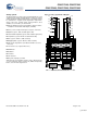
CY8C27143, CY8C27243 CY8C27443, CY8C27543, CY8C27643 Device Programmers CY3207ISSP In-System Serial Programmer (ISSP) All device programmers can be purchased from the Cypress Online Store. The CY3207ISSP is a production programmer. It includes protection circuitry and an industrial case that is more robust than the MiniProg in a production-programming environment. Note: CY3207ISSP needs special software and is not compatible with PSoC Programmer.
CY8C27143, CY8C27243 CY8C27443, CY8C27543, CY8C27643 Ordering Information The following table lists the CY8C27x43 PSoC device’s key package features and ordering codes. XRES Pin Analog Outputs Analog Inputs Digital I/O Pins Analog Blocks (Columns of 3) Digital Blocks (Rows of 4) Temperature Range Switch Mode Pump RAM (Bytes) Flash (Bytes) Package Ordering Code Table 47.
CY8C27143, CY8C27243 CY8C27443, CY8C27543, CY8C27643 RAM (Bytes) Switch Mode Pump Temperature Range Digital Blocks (Rows of 4) Analog Blocks (Columns of 3) Digital I/O Pins Analog Inputs Analog Outputs XRES Pin 44 Pin TQFP (Tape and Reel) CY8C27543-24AIT 16K 256 Yes -40C to +85C 8 12 40 12 4 Yes 48 Pin (300 Mil) SSOP CY8C27643-24PVI 16K 256 Yes -40C to +85C 8 12 44 12 4 Yes 48 Pin (300 Mil) SSOP (Tape and Reel) CY8C27643-24PVIT 16K 256 Yes -40C to +85C 8 12 44 12
CY8C27143, CY8C27243 CY8C27443, CY8C27543, CY8C27643 Document History Page Document Title: CY8C27143, CY8C27243, CY8C27443, CY8C27543, CY8C27643 PSoC® Programmable System-on-Chip Document Number: 38-12012 Revision ECN No. Submission Date Origin of Change Description of Change ** 127087 7/01/2003 New Silicon. *A 128780 7/29/2003 Engineering and New electrical spec additions, fix of Core Architecture links, corrections to NWJ. some text, tables, drawings, and format.
CY8C27143, CY8C27243 CY8C27443, CY8C27543, CY8C27643 Sales, Solutions, and Legal Information Worldwide Sales and Design Support Cypress maintains a worldwide network of offices, solution centers, manufacturer’s representatives, and distributors. To find the office closest to you, visit us at cypress.com/sales. Products PSoC Clocks & Buffers psoc.cypress.com clocks.cypress.com Wireless wireless.cypress.com Memories memory.cypress.com Image Sensors image.cypress.