
Specifications


CY8C24094, CY8C24794
CY8C24894, CY8C24994
Document Number: 38-12018 Rev. AH Page 8 of 64
8. Pin Information
This section describes, lists, and illustrates the CY8C24x94 PSoC device family pins and pinout configuration.
The CY8C24x94 PSoC devices are available in the following packages, all of which are shown on the following pages. Every port pin
(labeled with a “P”) is capable of Digital I/O. However, V
SS
, V
DD
, and XRES are not capable of Digital I/O.
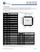
8.1 56-Pin Part Pinout
Notes
3. This part cannot be programmed with Reset mode; use Power Cycle mode when programming.
4. These are the ISSP pins, which are not High Z at POR. See the PSoC Technical Reference Manual for details.
Table 2. 56-Pin Part Pinout (QFN
[6]
) See LEGEND details and footnotes in Table 3 on page 9.
Pin
No.
Type
Name Description
Figure 3. CY8C24794 56-Pin PSoC Device
[3]
Digital Analog
1 I/O I, M P2[3] Direct switched capacitor block input
2 I/O I, M P2[1] Direct switched capacitor block input
3 I/O M P4[7]
4 I/O M P4[5]
5 I/O M P4[3]
6 I/O M P4[1]
7 I/O M P3[7]
8 I/O M P3[5]
9 I/O M P3[3]
10 I/O M P3[1]
11 I/O M P5[7]
12 I/O M P5[5]
13 I/O M P5[3]
14 I/O M P5[1]
15 I/O M P1[7] I
2
C serial clock (SCL)
16 I/O M P1[5] I
2
C serial data (SDA)
17 I/O M P1[3]
18 I/O M P1[1] I
2
C SCL, ISSP SCLK
[4]
19 Power V
SS
Ground connection
20 USB D+
21 USB D–
22 Power V
DD
Supply voltage
23 I/O P7[7]
24 I/O P7[0]
25 I/O M P1[0] I
2
C SDA, ISSP SDATA
[4]
26 I/O M P1[2]
27 I/O M P1[4] Optional external clock input (EXTCLK)
28 I/O M P1[6]
29 I/O M P5[0]
Pin
No.
Type
Name Description
30 I/O M P5[2]
Digital Analog
31 I/O M P5[4] 44 I/O M P2[6] External voltage reference (VREF) input
32 I/O M P5[6] 45 I/O I, M P0[0] Analog column mux input
33 I/O M P3[0] 46 I/O I, M P0[2] Analog column mux input
34 I/O M P3[2] 47 I/O I, M P0[4] Analog column mux input VREF
35 I/O M P3[4] 48 I/O I, M P0[6] Analog column mux input
36 I/O M P3[6] 49 Power V
DD
Supply voltage
37 I/O M P4[0] 50 Power V
SS
Ground connection
38 I/O M P4[2] 51 I/O I, M P0[7] Analog column mux input
39 I/O M P4[4] 52 I/O I/O, M P0[5] Analog column mux input and column output
40 I/O M P4[6] 53 I/O I/O, M P0[3] Analog column mux input and column output
41 I/O I, M P2[0] Direct switched capacitor block input 54 I/O I, M P0[1] Analog column mux input
42 I/O I, M P2[2] Direct switched capacitor block input 55 I/O M P2[7]
43 I/O M P2[4] External analog ground (AGND) input 56 I/O M P2[5]
QFN
(Top View )
A, I, M, P2[3]
A, I, M, P2[1]
M, P4[7]
M, P4[5]
M, P4[3]
M, P4[1]
M, P3[7]
M, P3[5]
M, P3[3]
M, P3[1]
M, P5[7]
M, P5[5]
M, P5[3]
M, P5[1]
1
2
3
4
5
6
7
8
9
10
11
12
13
14
M, I2C SCL, P1[7]
M, I2C SDA, P1[5]
M, P1[3]
M, I2C SCL, P1[1]
Vss
D+
D-
Vdd
P7[7]
P7[0]
M, I2C SDA, P1[0]
M, P1[2]
M, P1[4]
M, P1[6]
15
16
17
18
19
20
21
22
23
24
25
26
27
28
P2[4], M
P2[6], M
P0[0], A, I, M
P0[2], A, I, M
P0[4], A, I, M
P0[6], A, I, M
Vdd
Vss
P0[7], A, I, M
P0[5], A, IO, M
P0[3], A, IO, M
P0[1], A, I, M
P2[7], M
P2[5], M
43
44
45
46
47
48
49
50
51
52
53
54
55
56
P2[2], A, I, M
P2[0], A, I, M
P4[6], M
P4[4], M
P4[2], M
P4[0], M
P3[6], M
P3[4], M
P3[2], M
P3[0], M
P5[6], M
P5[4], M
P5[2], M
P5[0], M
42
41
40
39
38
37
36
35
34
33
32
31
30
29
EXTCLK,