CY8C24094, CY8C24794 CY8C24894, CY8C24994 PSoC® Programmable System-on-Chip™ PSoC® Programmable System-on-Chip 1. Features ■ ■ ■ ■ ■ XRES pin to support in-system serial programming (ISSP) and external reset control in CY8C24894 Powerful Harvard-architecture processor ❐ M8C processor speeds up to 24 MHz ❐ Two 8 × 8 multiply, 32-bit accumulate ❐ Low power at high speed ❐ Operating voltage: 3 V to 5.
CY8C24094, CY8C24794 CY8C24894, CY8C24994 3. Contents PSoC Functional Overview ................................................3 The PSoC Core .............................................................3 The Digital System ........................................................3 The Analog System .......................................................4 Additional System Resources .......................................5 PSoC Device Characteristics ........................................
CY8C24094, CY8C24794 CY8C24894, CY8C24994 4. PSoC Functional Overview The PSoC family consists of many devices with on-chip controllers. These devices are designed to replace multiple traditional MCU-based system components with one low-cost single-chip programmable component. A PSoC device includes configurable blocks of analog and digital logic, and programmable interconnect.
CY8C24094, CY8C24794 CY8C24894, CY8C24994 4.3 The Analog System The analog system is composed of six configurable blocks, each comprised of an opamp circuit allowing the creation of complex analog signal flows. Analog peripherals are very flexible and can be customized to support specific application requirements. Some of the more common PSoC analog functions (most available as user modules) are as follows. Figure 2.
CY8C24094, CY8C24794 CY8C24894, CY8C24994 4.4 Additional System Resources System resources provide additional capability useful to complete systems. Additional resources include a multiplier, decimator, low-voltage detection, and power-on reset (POR). Brief statements describing the merits of each resource follow. ■ ■ ■ Full speed USB (12 Mbps) with five configurable endpoints and 256 bytes of RAM. No external components required except for two series resistors.
CY8C24094, CY8C24794 CY8C24894, CY8C24994 5. Getting Started For in-depth information, along with detailed programming information, see the Technical Reference Manual for this PSoC device. For up-to-date ordering, packaging, and electrical specification information, see the latest PSoC device datasheets on the web at http://www.cypress.com. 5.1 Application Notes Cypress application notes are an excellent introduction to the wide variety of possible PSoC designs. 5.
CY8C24094, CY8C24794 CY8C24894, CY8C24994 read and write data memory, and read and write I/O registers. You can read and write CPU registers, set and clear breakpoints, and provide program run, halt, and step control. The debugger also allows you to create a trace buffer of registers and memory locations of interest. 6.1.4 Online Help System The online help system displays online, context-sensitive help.
CY8C24094, CY8C24794 CY8C24894, CY8C24994 8. Pin Information This section describes, lists, and illustrates the CY8C24x94 PSoC device family pins and pinout configuration. The CY8C24x94 PSoC devices are available in the following packages, all of which are shown on the following pages. Every port pin (labeled with a “P”) is capable of Digital I/O. However, VSS, VDD, and XRES are not capable of Digital I/O. 8.1 56-Pin Part Pinout Table 2.
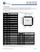
CY8C24094, CY8C24794 CY8C24894, CY8C24994 8.2 56-Pin Part Pinout (with XRES) Table 3. 56-Pin Part Pinout (QFN[6]) Figure 4. CY8C24894 56-Pin PSoC Device I/O M P5[2] No.
CY8C24094, CY8C24794 CY8C24894, CY8C24994 8.3 68-Pin Part Pinout The following 68-pin QFN part table and drawing is for the CY8C24994 PSoC device. Table 4. 68-Pin Part Pinout (QFN[7]) 44 45 46 Input M M M M M M M M M M M M P7[0] P1[0] P1[2] P1[4] P1[6] P5[0] P5[2] P5[4] P5[6] P3[0] P3[2] P3[4] P3[6] NC NC XRES Pin I2C SDA, ISSP SDATA[8] Optional EXTCLK No connection. Pin must be left floating. No connection. Pin must be left floating.
CY8C24094, CY8C24794 CY8C24894, CY8C24994 8.4 68-Pin Part Pinout (On-Chip Debug) The following 68-pin QFN part table and drawing is for the CY8C24094 OCD PSoC device. Note This part is only used for in-circuit debugging. It is NOT available for production. Table 5. 68-Pin Part Pinout (QFN[9]) M M M M M M M M M M M M P7[0] P1[0] P1[2] P1[4] P1[6] P5[0] P5[2] P5[4] P5[6] P3[0] P3[2] P3[4] P3[6] Pin Optional EXTCLK No.
CY8C24094, CY8C24794 CY8C24894, CY8C24994 8.5 100-Ball VFBGA Part Pinout The 100-ball VFBGA part is for the CY8C24994 PSoC device.
CY8C24094, CY8C24794 CY8C24894, CY8C24994 Figure 7.
CY8C24094, CY8C24794 CY8C24894, CY8C24994 8.6 100-Ball VFBGA Part Pinout (On-Chip Debug) The following 100-pin VFBGA part table and drawing is for the CY8C24094 OCD PSoC device. Note This part is only used for in-circuit debugging. It is NOT available for production. Description Pin No. Analog Name Digital Analog Pin No. Digital Table 7.
CY8C24094, CY8C24794 CY8C24894, CY8C24994 Figure 8.
CY8C24094, CY8C24794 CY8C24894, CY8C24994 8.7 100-Pin Part Pinout (On-Chip Debug) The 100-pin TQFP part is for the CY8C24094 OCD PSoC device. Note This part is only used for in-circuit debugging. It is NOT available for production. Description Pin No. Analog Name Digital Analog Pin No. Digital Table 8. 100-Pin Part Pinout (TQFP) Name Description 1 NC No connection. Pin must be left floating 51 I/O M P1[6] 2 NC No connection.
CY8C24094, CY8C24794 CY8C24894, CY8C24994 Document Number: 38-12018 Rev.
CY8C24094, CY8C24794 CY8C24894, CY8C24994 9. Register Reference This section lists the registers of the CY8C24x94 PSoC device family. For detailed register information, see the PSoC Technical Reference Manual. 9.1 Register Conventions 9.2 Register Mapping Tables The register conventions specific to this section are listed in the following table. The PSoC device has a total register address space of 512 bytes.
CY8C24094, CY8C24794 CY8C24894, CY8C24994 9.
CY8C24094, CY8C24794 CY8C24894, CY8C24994 9.
CY8C24094, CY8C24794 CY8C24894, CY8C24994 10. Electrical Specifications This section presents the DC and AC electrical specifications of the CY8C24x94 PSoC device family. For the most up-to-date electrical specifications, confirm that you have the most recent datasheet by visiting http://www.cypress.com. Specifications are valid for –40 °C TA 85 °C and TJ 100 °C, except where noted. Specifications for devices running at greater than 12 MHz are valid for –40 °C TA 70 °C and TJ 82 °C. Figure 10.
CY8C24094, CY8C24794 CY8C24894, CY8C24994 10.2 Operating Temperature Table 10. Operating Temperature Symbol TA TAUSB TJ Description Ambient temperature Ambient temperature using USB Junction temperature Min –40 –10 –40 Typ – – – Max +85 +85 +100 Units °C °C °C Notes The temperature rise from ambient to junction is package specific. See Thermal Impedance on page 44. The user must limit the power consumption to comply with this requirement. 10.3 DC Electrical Characteristics 10.3.
CY8C24094, CY8C24794 CY8C24894, CY8C24994 10.3.2 DC GPIO Specifications The following table lists guaranteed maximum and minimum specifications for the voltage and temperature ranges: 4.75 V to 5.25 V and –40 °C TA 85 °C, or 3.0 V to 3.6 V and –40 °C TA 85 °C, respectively. Typical parameters are measured at 5 V and 3.3 V at 25 °C and are for design guidance only. Table 12. DC GPIO Specifications Symbol Description Pull-up resistor RPU Pull-down resistor RPD High output level VOH Min 4 4 VDD – 1.
CY8C24094, CY8C24794 CY8C24894, CY8C24994 10.3.3 DC Full Speed USB Specifications The following table lists guaranteed maximum and minimum specifications for the voltage and temperature ranges: 4.75 V to 5.25 V and –10 C TA 85 °C, or 3.0 V to 3.6 V and –10 °C TA 85 °C, respectively. Typical parameters are measured at 5 V and 3.3 V at 25 °C and are for design guidance only. Table 13.
CY8C24094, CY8C24794 CY8C24894, CY8C24994 10.3.4 DC Operational Amplifier Specifications The following tables list guaranteed maximum and minimum specifications for the voltage and temperature ranges: 4.75 V to 5.25 V and –40 °C TA 85 °C, or 3.0 V to 3.6 V and –40 °C TA 85 °C, respectively. Typical parameters are measured at 5 V and 3.3 V at 25 °C and are for design guidance only.
CY8C24094, CY8C24794 CY8C24894, CY8C24994 Table 15. 3.3-V DC Operational Amplifier Specifications Symbol VOSOA Min Typ Max Units TCVOSOA IEBOA CINOA Description Input offset voltage (absolute value) Power = low, Opamp bias = high Power = medium, Opamp bias = high Power = high, Opamp bias = high Average input offset voltage drift Input leakage current (port 0 analog pins) Input capacitance (port 0 analog pins) – – – – – – 1.65 1.32 – 7.0 20 4.5 10 8 – 35.0 – 9.
CY8C24094, CY8C24794 CY8C24894, CY8C24994 10.3.6 DC Analog Output Buffer Specifications The following tables list guaranteed maximum and minimum specifications for the voltage and temperature ranges: 4.75 V to 5.25 V and –40 °C TA 85 °C, or 3.0 V to 3.6 V and –40 °C TA 85 °C, respectively. Typical parameters are measured at 5 V and 3.3 V at 25 °C and are for design guidance only. Table 17.
CY8C24094, CY8C24794 CY8C24894, CY8C24994 Table 18. 3.
CY8C24094, CY8C24794 CY8C24894, CY8C24994 10.3.7 DC Analog Reference Specifications The following tables list guaranteed maximum and minimum specifications for the voltage and temperature ranges: 4.75 V to 5.25 V and –40 °C TA 85 °C, or 3.0 V to 3.6 V and –40 °C TA 85 °C, respectively. Typical parameters apply to 5 V and 3.3 V at 25 °C and are for design guidance only. The guaranteed specifications for RefHI and RefLo are measured through the Analog Continuous Time PSoC blocks.
CY8C24094, CY8C24794 CY8C24894, CY8C24994 Table 19. 5-V DC Analog Reference Specifications (continued) Reference ARF_CR [5:3] 0b010 Reference Power Settings RefPower = high Opamp bias = high RefPower = high Opamp bias = low 0b011 Reference Description VREFHI Ref High VDD Min Typ Max Units VDD – 0.037 VDD – 0.007 VDD V VAGND AGND VDD/2 VREFLO Ref Low VSS VSS VSS + 0.005 VSS + 0.029 V VREFHI Ref High VDD VDD – 0.034 VDD – 0.006 VDD V VDD/2 – 0.036 VDD/2 – 0.001 VDD/2 + 0.
CY8C24094, CY8C24794 CY8C24894, CY8C24994 Table 19. 5-V DC Analog Reference Specifications (continued) Reference ARF_CR [5:3] 0b101 Reference Power Settings RefPower = high Opamp bias = high RefPower = high Opamp bias = low 0b110 Reference Description Min Typ Max Units P2[4] + 1.218 P2[4] + 1.291 P2[4] + 1.354 V P2[4] P2[4] P2[4] – VREFHI Ref High P2[4] + Bandgap (P2[4] = VDD/2) VAGND AGND P2[4] VREFLO Ref Low P2[4] – Bandgap (P2[4] = VDD/2) P2[4] – 1.335 P2[4] – 1.
CY8C24094, CY8C24794 CY8C24894, CY8C24994 Table 20. 3.3-V DC Analog Reference Specifications Reference ARF_CR [5:3] 0b000 Reference Power Settings RefPower = high Opamp bias = high Description VREFHI Ref High VDD/2 + Bandgap VAGND AGND VREFLO Ref Low VREFHI Min Typ Max Units V VDD/2 VDD/2 – Bandgap VDD/2 – 1.346 VDD/2 – 1.292 VDD/2 – 1.208 V Ref High VDD/2 + Bandgap V VAGND AGND VDD/2 VDD/2 + 1.196 VDD/2 + 1.292 VDD/2 + 1.374 VDD/2 – 0.029 VDD/2 VDD/2 + 0.
CY8C24094, CY8C24794 CY8C24894, CY8C24994 Table 20. 3.3-V DC Analog Reference Specifications (continued) Reference ARF_CR [5:3] Reference Power Settings Symbol Reference Description Min Typ Max Units 0b011 All power settings. – Not allowed for 3.3 V. – – – – – – 0b100 All power settings. – Not allowed for 3.3 V. – – – – – – 0b101 RefPower = high Opamp bias = high VREFHI Ref High P2[4] + Bandgap (P2[4] = VDD/2) P2[4] + 1.214 P2[4] + 1.291 P2[4] + 1.
CY8C24094, CY8C24794 CY8C24894, CY8C24994 10.3.8 DC Analog PSoC Block Specifications The following table lists guaranteed maximum and minimum specifications for the voltage and temperature ranges: 4.75 V to 5.25 V and –40 °C TA 85 °C, or 3.0 V to 3.6 V and –40 °C TA 85 °C, respectively. Typical parameters are measured at 5 V and 3.3 V at 25 °C and are for design guidance only. Table 21.
CY8C24094, CY8C24794 CY8C24894, CY8C24994 10.3.10 DC Programming Specifications The following table lists guaranteed maximum and minimum specifications for the voltage and temperature ranges: 4.75 V to 5.25 V and –40 °C TA 85 °C, or 3.0 V to 3.6 V and –40 °C TA 85 °C, respectively. Typical parameters are measured at 5 V and 3.3 V at 25 °C and are for design guidance only. Table 23. DC Programming Specifications Symbol VDDP Description VDD for programming and erase Min 4.5 Typ 5 Max 5.
CY8C24094, CY8C24794 CY8C24894, CY8C24994 10.4 AC Electrical Characteristics 10.4.1 AC Chip-Level Specifications The following table lists guaranteed maximum and minimum specifications for the voltage and temperature ranges: 4.75 V to 5.25 V and –40 C TA 85 C, or 3.0 V to 3.6 V and –40 C TA 85 C, respectively. Typical parameters are measured at 5 V and 3.3 V at 25 C and are for design guidance only. Table 25.
CY8C24094, CY8C24794 CY8C24894, CY8C24994 10.4.2 AC GPIO Specifications The following table lists guaranteed maximum and minimum specifications for the voltage and temperature ranges: 4.75 V to 5.25 V and –40 °C TA 85 °C, or 3.0 V to 3.6 V and –40 °C TA 85 °C, respectively. Typical parameters are measured at 5 V and 3.3 V at 25 °C and are for design guidance only. Table 26.
CY8C24094, CY8C24794 CY8C24894, CY8C24994 10.4.4 AC Operational Amplifier Specifications The following tables list guaranteed maximum and minimum specifications for the voltage and temperature ranges: 4.75 V to 5.25 V and –40 °C TA 85 °C, or 3.0 V to 3.6 V and –40 °C TA 85 °C, respectively. Typical parameters are measured at 5 V and 3.3 V at 25 °C and are for design guidance only. Settling times, slew rates, and gain bandwidth are based on the analog continuous time PSoC block.
CY8C24094, CY8C24794 CY8C24894, CY8C24994 When bypassed by a capacitor on P2[4], the noise of the analog ground signal distributed to each block is reduced by a factor of up to 5 (14 dB). This is at frequencies above the corner frequency defined by the on-chip 8.1 K resistance and the external capacitor. Figure 12. Typical AGND Noise with P2[4] Bypass nV/rtHz 10000 0 0.01 0.1 1.0 10 1000 100 0.001 0.01 0.
CY8C24094, CY8C24794 CY8C24894, CY8C24994 10.4.5 AC Low Power Comparator Specifications The following table lists guaranteed maximum and minimum specifications for the voltage and temperature ranges: 4.75 V to 5.25 V and –40 °C TA 85 °C or 3.0 V to 3.6 V and –40 °C TA 85 °C, respectively. Typical parameters are measured at 5 V at 25 °C and are for design guidance only. Table 30.
CY8C24094, CY8C24794 CY8C24894, CY8C24994 Table 31. AC Digital Block Specifications (continued) Function Transmitter Receiver Description Input clock frequency VDD 4.75 V, 2 stop bits VDD 4.75 V, 1 stop bit VDD < 4.75 V Input clock frequency VDD 4.75 V, 2 stop bits VDD 4.75 V, 1 stop bit VDD < 4.75 V Min Typ Max Unit – – – – – – 49.92 24.6 24.6 MHz MHz MHz – – – – – – 49.92 24.6 24.6 MHz MHz MHz Notes The baud rate is equal to the input clock frequency divided by 8.
CY8C24094, CY8C24794 CY8C24894, CY8C24994 Table 34. 3.3-V AC Analog Output Buffer Specifications Symbol tROB tSOB SRROB SRFOB BWOBSS BWOBLS Description Rising settling time to 0.1%, 1 V Step, 100 pF load Power = low Power = high Falling settling time to 0.
CY8C24094, CY8C24794 CY8C24894, CY8C24994 10.4.10 AC I2C Specifications The following table lists guaranteed maximum and minimum specifications for the voltage and temperature ranges: 4.75 V to 5.25 V and –40 °C TA 85 °C, or 3.0 V to 3.6 V and –40 °C TA 85 °C, respectively. Typical parameters are measured at 5 V and 3.3 V at 25 °C and are for design guidance only. Table 36.
CY8C24094, CY8C24794 CY8C24894, CY8C24994 10.5 Thermal Impedance Table 37. Thermal Impedances per Package Typical JA [29] 12.93 °C/W 13.05 °C/W 65 °C/W 51 °C/W Package 56-Pin QFN[30] 68-Pin QFN[30] 100-Ball VFBGA 100-Pin TQFP 10.6 Solder Reflow Peak Specifications Table 38 shows the solder reflow temperature limits that must not be exceeded. Table 38.
CY8C24094, CY8C24794 CY8C24894, CY8C24994 11. Development Tool Selection 11.1 Software ■ 28-Pin CY8C27443-24PXI PDIP PSoC device sample 11.1.1 PSoC Designer ■ PSoC Designer software CD At the core of the PSoC development software suite is PSoC Designer, used to generate PSoC firmware applications. PSoC Designer is available free of charge at http://www.cypress.com and includes a free C compiler. ■ Getting Started guide ■ USB 2.0 cable 11.1.
CY8C24094, CY8C24794 CY8C24894, CY8C24994 ■ Getting Started guide ■ CY3207 programmer unit ■ USB 2.0 cable ■ PSoC ISSP software CD 11.4.2 CY3207ISSP In-System Serial Programmer (ISSP) ■ 110 ~ 240 V power supply, Euro-Plug adapter The CY3207ISSP is a production programmer. It includes protection circuitry and an industrial case that is more robust than the MiniProg in a production-programming environment. ■ USB 2.
CY8C24094, CY8C24794 CY8C24894, CY8C24994 12.
CY8C24094, CY8C24794 CY8C24894, CY8C24994 13. Packaging Dimensions This section illustrates the package specification for the CY8C24x94 PSoC devices, along with the thermal impedance for the package and solder reflow peak temperatures. Important Note Emulation tools may require a larger area on the target PCB than the chip's footprint. For a detailed description of the emulation tools' dimensions, refer to the emulator pod dimension drawings at http://www.cypress.com/design/MR10161. Figure 15.
CY8C24094, CY8C24794 CY8C24894, CY8C24994 Figure 16. 56-Pin (8 × 8 mm) QFN SOLDERABLE EXPOSED PAD 001-12921 *B Figure 17. 56-Pin QFN (8 × 8 × 0.9 mm) – Sawn 001-53450 *C Document Number: 38-12018 Rev.
CY8C24094, CY8C24794 CY8C24894, CY8C24994 Figure 18. 68-Pin Sawn QFN (8 × 8 mm × 0.90 mm) 001-09618 *E Document Number: 38-12018 Rev.
CY8C24094, CY8C24794 CY8C24894, CY8C24994 Figure 19. 100-Ball (6 × 6 mm) VFBGA 51-85209 *D Document Number: 38-12018 Rev.
CY8C24094, CY8C24794 CY8C24894, CY8C24994 Figure 20. 100-Pin (14 × 14 × 1.4 mm) TQFP 51-85048 *G Important Note ■ For information on the preferred dimensions for mounting QFN packages, see the Application Note, Application Notes for Surface Mount Assembly of Amkor's MicroLeadFrame (MLF) Packages available at http://www.amkor.com. ■ Pinned vias for thermal conduction are not required for the low power PSoC device. Document Number: 38-12018 Rev.
CY8C24094, CY8C24794 CY8C24894, CY8C24994 14. Acronyms 14.1 Acronyms Used The following table lists the acronyms that are used in this document.
CY8C24094, CY8C24794 CY8C24894, CY8C24994 15. Document Conventions 15.1 Units of Measure Symbol °C dB fF kHz k MHz A s V mA mm ms Unit of Measure degree Celsius decibels femtofarad kilohertz kilohms megahertz microampere microsecond microvolt milliampere millimeter millisecond Symbol mV nA ns nV pA pF ps % rt-Hz V W Unit of Measure millivolt nanoampere nanosecond nanovolt ohms picoampere picofarad picosecond percent root hertz volt watt 15.
CY8C24094, CY8C24794 CY8C24894, CY8C24994 16. Glossary (continued) block 1. A functional unit that performs a single function, such as an oscillator. 2. A functional unit that may be configured to perform one of several functions, such as a digital PSoC block or an analog PSoC block. buffer 1. A storage area for data that is used to compensate for a speed difference, when transferring data from one device to another.
CY8C24094, CY8C24794 CY8C24894, CY8C24994 16. Glossary (continued) external reset (XRES) An active high signal that is driven into the PSoC device. It causes all operation of the CPU and blocks to stop and return to a pre-defined state. flash An electrically programmable and erasable, non-volatile technology that provides users with the programmability and data storage of EPROMs, plus in-system erasability. Non-volatile means that the data is retained when power is off.
CY8C24094, CY8C24794 CY8C24894, CY8C24994 16. Glossary (continued) modulator A device that imposes a signal on a carrier. noise 1. A disturbance that affects a signal and that may distort the information carried by the signal. 2. The random variations of one or more characteristics of any entity such as voltage, current, or data. oscillator A circuit that may be crystal controlled and is used to generate a clock frequency. parity A technique for testing transmitting data.
CY8C24094, CY8C24794 CY8C24894, CY8C24994 16. Glossary (continued) SRAM An acronym for static random access memory. A memory device allowing users to store and retrieve data at a high rate of speed. The term static is used because, after a value has been loaded into an SRAM cell, it remains unchanged until it is explicitly altered or until power is removed from the device. SROM An acronym for supervisory read only memory.
CY8C24094, CY8C24794 CY8C24894, CY8C24994 17. Errata This section describes the errata for the CY8C24x94 device. Details include errata trigger conditions, scope of impact, available workaround, and silicon revision applicability. Contact your local Cypress Sales Representative if you have questions. Part Numbers Affected Part Number CY8C24x94 CY8C24x94 Errata Summary The following table defines the errata applicability to available devices. Items Part Number 1.
CY8C24094, CY8C24794 CY8C24894, CY8C24994 ■ WORKAROUND To prevent an invalid Flash read, a dummy read from each Flash page must occur before use of the pages. A delay of 5 µs must occur after the dummy read and before a real read. The dummy reads occurs as soon as possible and must be located in Flash page 0 before a read from any other Flash page. An example for reading a byte of memory from each Flash page is listed below. Placed it in boot.tpl and boot.asm immediately after the ‘start:’ label.
CY8C24094, CY8C24794 CY8C24894, CY8C24994 18. Document History Page Document Title: CY8C24094, CY8C24794, CY8C24894, CY8C24994 PSoC® Programmable System-on-Chip™ Document Number: 38-12018 Revision ECN Orig. of Change Submission Date Description of Change ** 133189 NWJ 01/27/2004 *A 251672 SFV See ECN First Preliminary datasheet. Changed title to encompass only the CY8C24794 because the CY8C24494 and CY8C24694 are not being offered by Cypress.
CY8C24094, CY8C24794 CY8C24894, CY8C24994 18. Document History Page (continued) Document Title: CY8C24094, CY8C24794, CY8C24894, CY8C24994 PSoC® Programmable System-on-Chip™ Document Number: 38-12018 *N 2708135 BRW 05/18/2009 Added Note in the Pin Information section on page 8. Removed reference to Hi-Tech Lite Compiler in the section Development Tools Selection on page 42.
CY8C24094, CY8C24794 CY8C24894, CY8C24994 18. Document History Page (continued) Document Title: CY8C24094, CY8C24794, CY8C24894, CY8C24994 PSoC® Programmable System-on-Chip™ Document Number: 38-12018 AD 3503402 PMAD 01/20/2012 Updated VOH and VOL section in Table 12. AE 3545509 PSAI 03/08/2012 Updated link to 'Technical reference Manual'. AF 3862667 CSAI 01/09/2013 Updated Ordering Information (Updated part numbers).
CY8C24094, CY8C24794 CY8C24894, CY8C24994 19. Sales, Solutions, and Legal Information Worldwide Sales and Design Support Cypress maintains a worldwide network of offices, solution centers, manufacturer’s representatives, and distributors. To find the office closest to you, visit us at Cypress Locations. PSoC® Solutions Products Automotive cypress.com/go/automotive Clocks & Buffers cypress.com/go/clocks Interface cypress.com/go/interface Lighting & Power Control cypress.com/go/powerpsoc cypress.