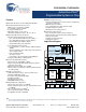
CY8C24223A, CY8C24423A Automotive PSoC® Programmable System-on-Chip Features ■ Automotive Electronics Council (AEC) Q100 qualified ■ Powerful Harvard-architecture processor ❐ M8C processor speeds up to 24 MHz ❐ 8 × 8 multiply, 32-bit accumulate ❐ Low power at high speed ❐ Operating voltage: 3.0 V to 5.
CY8C24223A, CY8C24423A Contents PSoC Functional Overview .............................................. 3 PSoC Core .................................................................. 3 Digital System ............................................................. 3 Analog System ............................................................ 4 Additional System Resources ..................................... 5 PSoC Device Characteristics ...................................... 5 Getting Started .................
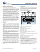
CY8C24223A, CY8C24423A The PSoC family consists of many programmable system-on-chips with on-chip Controller devices. These devices are designed to replace multiple traditional microcontroller unit (MCU)-based system components with one, low cost single-chip programmable device. PSoC devices include configurable blocks of analog and digital logic, and programmable interconnects.
CY8C24223A, CY8C24423A The analog system is composed of six configurable blocks, each comprised of an opamp circuit allowing the creation of complex analog signal flows. Analog peripherals are very flexible and can be customized to support specific application requirements.
CY8C24223A, CY8C24423A Additional System Resources System resources, some of which have been previously listed, provide additional capability useful for complete systems. Additional resources include a multiplier, decimator, low voltage detection, and power-on reset (POR). Brief statements describing the merits of each system resource follow: ■ Digital clock dividers provide three customizable clock frequencies for use in applications. The clocks can be routed to both the digital and analog systems.
CY8C24223A, CY8C24423A Getting Started ■ Built-in debugger For in-depth information, along with detailed programming details, see the PSoC® Technical Reference Manual. ■ In-circuit emulation For up-to-date ordering, packaging, and electrical specification information, see the latest PSoC device datasheets on the web. Application Notes Cypress application notes are an excellent introduction to the wide variety of possible PSoC designs.
CY8C24223A, CY8C24423A subsystem has its own context-sensitive help. This system also provides tutorials and links to FAQs and an online support Forum to aid the designer. In-Circuit Emulator A low-cost, high-functionality in-circuit emulator (ICE) is available for development support. This hardware can program single devices. The emulator consists of a base unit that connects to the PC using a USB port. The base unit is universal and operates with all PSoC devices.
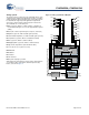
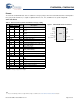
CY8C24223A, CY8C24423A Pinouts The automotive CY8C24x23A PSoC device is available in a variety of packages which are listed and illustrated in the following tables. Every port pin (labeled with a “P”) is capable of digital I/O. However, VSS, VDD, and XRES are not capable of digital I/O. 20-Pin Part Pinout Table 2. 20-Pin Part Pinout (Shrink Small-Outline Package (SSOP)) Pin No.
CY8C24223A, CY8C24423A 28-Pin Part Pinout Table 3. 28-Pin Part Pinout (SSOP) Type Pin Pin Description No.
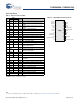
CY8C24223A, CY8C24423A Registers Register Conventions Register Mapping Tables This section lists the registers of the automotive CY8C24x23A PSoC device. For detailed register information, refer to the PSoC Technical Reference Manual. The register conventions specific to this section are listed in the following table. The PSoC device has a total register address space of 512 bytes. The register space is referred to as I/O space and is divided into two banks, bank 0 and bank 1.
CY8C24223A, CY8C24423A Table 5.
CY8C24223A, CY8C24423A Table 6.
CY8C24223A, CY8C24423A Electrical Specifications This section presents the DC and AC electrical specifications of the automotive CY8C24x23A PSoC devices. For the latest electrical specifications, visit http://www.cypress.com. Specifications are valid for –40 °C TA 85 °C and TJ 100 °C, except where noted. Refer to Table 21 on page 27 for the electrical specifications of the IMO using slow IMO (SLIMO) mode. Figure 5. Voltage versus CPU Frequency Figure 6. IMO Frequency Trim Options 5.25 5.
CY8C24223A, CY8C24423A Absolute Maximum Ratings Exceeding maximum ratings may shorten the useful life of the device. User guidelines are not tested. Table 7.
CY8C24223A, CY8C24423A DC Electrical Characteristics DC Chip-Level Specifications Table 9 lists the guaranteed maximum and minimum specifications for the voltage and temperature ranges: 4.75 V to 5.25 V and –40 °C TA 85 °C, 3.0 V to 3.6 V and –40 °C TA 85 °C, respectively. Typical parameters apply to 5 V and 3.3 V at 25 °C and are for design guidance only. Table 9. DC Chip-Level Specifications Symbol Description VDD Supply voltage Min 3.0 Typ – Max 5.
CY8C24223A, CY8C24423A DC GPIO Specifications Table 10 lists the guaranteed maximum and minimum specifications for the voltage and temperature ranges: 4.75 V to 5.25 V and –40 °C TA 85 °C, 3.0 V to 3.6 V and –40 °C TA 85 °C, respectively. Typical parameters apply to 5 V and 3.3 V at 25 °C and are for design guidance only. Table 10. DC GPIO Specifications Min Typ Max Units RPU Symbol Pull-up resistor Description 4 5.6 8 k Notes RPD Pull-down resistor 4 5.
CY8C24223A, CY8C24423A DC Operational Amplifier Specifications The following tables list the guaranteed maximum and minimum specifications for the voltage and temperature ranges: 4.75 V to 5.25 V and –40 °C TA 85 °C, 3.0 V to 3.6 V and –40 °C TA 85 °C, respectively. Typical parameters apply to 5 V and 3.3 V at 25 °C and are for design guidance only. The operational amplifier is a component of both the analog CT PSoC blocks and the analog SC PSoC blocks.
CY8C24223A, CY8C24423A Table 12. 3.3-V DC Operational Amplifier Specifications Symbol VOSOA Description Input offset voltage (absolute value) Power = low, Opamp bias = high Power = medium, Opamp bias = high Power = high, Opamp bias = high Min Typ Max Units – – – 1.65 1.32 – 10 8 – mV mV mV TCVOSOA Average input offset voltage drift – 7.0 35.0 V/°C Notes Power = high, Opamp bias = high is not allowed. IEBOA Input leakage current (Port 0 analog pins) – 20 – pA Gross tested to 1 A.
CY8C24223A, CY8C24423A DC Analog Output Buffer Specifications The following tables list the guaranteed maximum and minimum specifications for the voltage and temperature ranges: 4.75 V to 5.25 V and –40 °C TA 85 °C, 3.0 V to 3.6 V and –40 °C TA 85 °C, respectively. Typical parameters apply to 5 V and 3.3 V at 25 °C and are for design guidance only. Table 14.
CY8C24223A, CY8C24423A DC Analog Reference Specifications The following tables list the guaranteed maximum and minimum specifications for the voltage and temperature ranges: 4.75 V to 5.25 V and –40 °C TA 85 °C, 3.0 V to 3.6 V and –40 °C TA 85 °C, respectively. Typical parameters apply to 5 V and 3.3 V at 25 °C and are for design guidance only. The guaranteed specifications are measured through the analog continuous time PSoC blocks.
CY8C24223A, CY8C24423A Table 16.
CY8C24223A, CY8C24423A Table 16.
CY8C24223A, CY8C24423A Table 17. 3.
CY8C24223A, CY8C24423A Table 17. 3.3-V DC Analog Reference Specifications (continued) Reference ARF_CR [5:3] Reference Power Settings Symbol Reference Description Min Typ Max Units – – – – P2[4] + 1.211 P2[4] + 1.285 P2[4] + 1.348 V P2[4] P2[4] P2[4] – 0b100 All power settings Not allowed at 3.3 V – – 0b101 RefPower = high Opamp bias = high VREFHI Ref High VAGND AGND VREFLO Ref Low P2[4] – Bandgap (P2[4] = VDD/2) P2[4] – 1.354 P2[4] – 1.290 P2[4] – 1.
CY8C24223A, CY8C24423A DC POR and LVD Specifications Table 19 lists the guaranteed maximum and minimum specifications for the voltage and temperature ranges: 4.75 V to 5.25 V and –40 °C TA 85 °C, 3.0 V to 3.6 V and –40 °C TA 85 °C, respectively. Typical parameters apply to 5 V and 3.3 V at 25 °C and are for design guidance only. Note The bits PORLEV and VM in the following table refer to bits in the VLT_CR register.
CY8C24223A, CY8C24423A DC Programming Specifications Table 20 lists the guaranteed maximum and minimum specifications for the voltage and temperature ranges: 4.75 V to 5.25 V and –40 °C TA 85 °C, 3.0 V to 3.6 V and –40 °C TA 85 °C, respectively. Typical parameters apply to 5 V and 3.3 V at 25 °C and are for design guidance only. Table 20. DC Programming Specifications Symbol VDDP Description VDD for programming and erase Min 4.5 Typ 5.0 Max 5.5 VDDLV Low VDD for verify 3.0 3.1 3.
CY8C24223A, CY8C24423A AC Electrical Characteristics AC Chip-Level Specifications Table 21 lists the guaranteed maximum and minimum specifications for the voltage and temperature ranges: 4.75 V to 5.25 V and –40 °C TA 85 °C, 3.0 V to 3.6 V and –40 °C TA 85 °C, respectively. Typical parameters apply to 5 V and 3.3 V at 25 °C and are for design guidance only. Table 21. AC Chip-Level Specifications Symbol FIMO24 Description IMO frequency for 24 MHz Min 22.8[13] Typ 24 Max 25.
CY8C24223A, CY8C24423A Figure 7. PLL Lock Timing Diagram PLL Enable t T PLLSLEW 24 MHz FPLL PLL Gain 0 Figure 8. PLL Lock for Low Gain Setting Timing Diagram PLL Enable t PLLSLEWLOW T 24 MHz FPLL PLL Gain 1 Figure 9. External Crystal Oscillator Startup Timing Diagram 32K Select 32 kHz t OS T F32K2 Document Number: 001-52469 Rev.
CY8C24223A, CY8C24423A AC GPIO Specifications Table 22 lists the guaranteed maximum and minimum specifications for the voltage and temperature ranges: 4.75 V to 5.25 V and –40 °C TA 85 °C, 3.0 V to 3.6 V and –40 °C TA 85 °C, respectively. Typical parameters apply to 5 V and 3.3 V at 25 °C and are for design guidance only. Table 22. AC GPIO Specifications Symbol Description Min Typ Max [16] Units Notes MHz Normal strong mode FGPIO GPIO operating frequency 0 – 12.
CY8C24223A, CY8C24423A AC Operational Amplifier Specifications The following tables list the guaranteed maximum and minimum specifications for the voltage and temperature ranges: 4.75 V to 5.25 V and –40 °C TA 85 °C, 3.0 V to 3.6 V and –40 °C TA 85 °C, respectively. Typical parameters apply to 5 V and 3.3 V at 25 °C and are for design guidance only. Settling times, slew rates, and gain bandwidth are based on the analog CT PSoC block. Power = high and Opamp bias = high is not allowed at 3.3 V.
CY8C24223A, CY8C24423A When bypassed by a capacitor on P2[4], the noise of the analog ground signal distributed to each block is reduced by a factor of up to 5 (14 dB). This is at frequencies above the corner frequency defined by the on-chip 8.1 k resistance and the external capacitor. Figure 11. Typical AGND Noise with P2[4] Bypass nV/rtHz 10000 0 0.01 0.1 1.0 10 1000 100 0.001 0.01 0.
CY8C24223A, CY8C24423A AC Low Power Comparator Specifications Table 25 lists the guaranteed maximum and minimum specifications for the voltage and temperature ranges: 4.75 V to 5.25 V and –40 °C TA 85 °C, 3.0 V to 3.6 V and –40 °C TA 85 °C, respectively. Typical parameters apply to 5 V and 3.3 V at 25 °C and are for design guidance only. Table 25.
CY8C24223A, CY8C24423A AC Analog Output Buffer Specifications The following tables list the guaranteed maximum and minimum specifications for the voltage and temperature ranges: 4.75 V to 5.25 V and –40 °C TA 85 °C, 3.0 V to 3.6 V and –40 °C TA 85 °C, respectively. Typical parameters apply to 5 V and 3.3 V at 25 °C and are for design guidance only. Table 27. 5-V AC Analog Output Buffer Specifications Symbol Description Min Typ Max Units tROB Rising settling time to 0.
CY8C24223A, CY8C24423A AC External Clock Specifications The following tables list the guaranteed maximum and minimum specifications for the voltage and temperature ranges: 4.75 V to 5.25 V and –40 °C TA 85 °C, 3.0 V to 3.6 V and –40 °C TA 85 °C, respectively. Typical parameters apply to 5 V and 3.3 V at 25 °C and are for design guidance only. Table 29. 5 V AC External Clock Specifications Symbol Description Min Typ Max Units FOSCEXT Frequency 0.093 – 24.6 MHz – High period 20.
CY8C24223A, CY8C24423A AC I2C Specifications Table 32 lists the guaranteed maximum and minimum specifications for the voltage and temperature ranges: 4.75 V to 5.25 V and –40 °C TA 85 °C, 3.0 V to 3.6 V and –40 °C TA 85 °C, respectively. Typical parameters apply to 5 V and 3.3 V at 25 °C and are for design guidance only. Table 32.
CY8C24223A, CY8C24423A Packaging Information This section illustrates the packaging specifications for the automotive CY8C24x23A PSoC device, along with the thermal impedances for the package and the typical package capacitance on crystal pins. Important Note Emulation tools may require a larger area on the target PCB than the chip’s footprint. For a detailed description of the emulation tools’ dimensions, refer to the emulator pod drawings at http://www.cypress.com. Packaging Dimensions Figure 14.
CY8C24223A, CY8C24423A Figure 15. 28-Pin (210-Mil) SSOP 51-85079 *E Thermal Impedances Solder Reflow Specifications Table 33. Thermal Impedances per Package Table 35 shows the solder reflow temperature limits that must not be exceeded. Typical JA [24] Package 20-pin SSOP 117 °C/W 28-pin SSOP 101 °C/W Capacitance on Crystal Pins Table 35.
CY8C24223A, CY8C24423A Figure 16. 20-Pin SSOP Carrier Tape Drawing 51-51101 *C Document Number: 001-52469 Rev.
CY8C24223A, CY8C24423A Figure 17. 28-Pin SSOP Carrier Tape Drawing 51-51100 *C Table 36. Tape and Reel Specifications Package Cover Tape Width (mm) Hub Size (inches) Minimum Leading Empty Pockets 20-Pin SSOP 28-Pin SSOP 13.3 13.3 4 7 42 42 Document Number: 001-52469 Rev.
CY8C24223A, CY8C24423A Development Tool Selection This section presents the development tools available for the CY8C24x23A family. Software PSoC Designer At the core of the PSoC development software suite is PSoC Designer, used to generate PSoC firmware applications. PSoC Designer is available free of charge at http://www.cypress.com and includes a free C compiler. Evaluation Tools All evaluation tools can be purchased from the Cypress Online Store.
CY8C24223A, CY8C24423A Note CY3207ISSP needs special software and is not compatible with PSoC Programmer. This software is free and can be downloaded from http://www.cypress.com. The kit includes: ■ CY3207 programmer unit ■ PSoC ISSP software CD ■ 110 ~ 240-V power supply, Euro-Plug adapter ■ USB 2.0 cable Accessories (Emulation and Programming) Table 37.
CY8C24223A, CY8C24423A Ordering Information The following table lists the automotive CY8C24x23A PSoC device group’s key package features and ordering codes.
CY8C24223A, CY8C24423A Reference Information Acronyms The following table lists the acronyms that are used in this document. Table 39.
CY8C24223A, CY8C24423A Document Conventions Units of Measure The following table lists the units of measure that are used in this document. Table 40.
CY8C24223A, CY8C24423A Glossary (continued) bias 1. A systematic deviation of a value from a reference value. 2. The amount by which the average of a set of values departs from a reference value. 3. The electrical, mechanical, magnetic, or other force (field) applied to a device to establish a reference level to operate the device. block 1. A functional unit that performs a single function, such as an oscillator. 2.
CY8C24223A, CY8C24423A Glossary (continued) duty cycle The relationship of a clock period high time to its low time, expressed as a percent. emulator Duplicates (provides an emulation of) the functions of one system with a different system, so that the second system appears to behave like the first system. external reset (XRES) An active high signal that is driven into the PSoC device. It causes all operation of the CPU and blocks to stop and return to a pre-defined state.
CY8C24223A, CY8C24423A Glossary (continued) microcontroller An integrated circuit chip that is designed primarily for control systems and products. In addition to a CPU, a microcontroller typically includes memory, timing circuits, and I/O circuitry. The reason for this is to permit the realization of a controller with a minimal quantity of chips, thus achieving maximal possible miniaturization. This in turn, reduces the volume and the cost of the controller.
CY8C24223A, CY8C24423A Glossary (continued) shift register A memory storage device that sequentially shifts a word either left or right to output a stream of serial data. slave device A device that allows another device to control the timing for data exchanges between two devices. Or when devices are cascaded in width, the slave device is the one that allows another device to control the timing of data exchanges between the cascaded devices and an external interface.
CY8C24223A, CY8C24423A Document History Page Document Title: CY8C24223A, CY8C24423A Automotive PSoC® Programmable System-on-Chip Document Number: 001-52469 Revision ECN Orig. of Change Submission Date ** 2678061 VIVG/PYRS 03/24/09 New data sheet for Automotive A-Grade *A 2685606 SHEA 04/08/09 Minor ECN to correct the spec number in Document History.
CY8C24223A, CY8C24423A Sales, Solutions, and Legal Information Worldwide Sales and Design Support Cypress maintains a worldwide network of offices, solution centers, manufacturer’s representatives, and distributors. To find the office closest to you, visit us at Cypress Locations. Products Automotive Clocks & Buffers Interface Lighting & Power Control PSoC Solutions cypress.com/go/automotive psoc.cypress.com/solutions cypress.com/go/clocks PSoC 1 | PSoC 3 | PSoC 5 cypress.com/go/interface cypress.
Mouser Electronics Authorized Distributor Click to View Pricing, Inventory, Delivery & Lifecycle Information: Cypress Semiconductor: CY8C24423A-24PVXA CY8C24423A-24PVXAT CY8C24223A-24PVXAT CY8C24223A-24PVXA