
User manual

CY8C24223A, CY8C24423A
Document Number: 38-12029 Rev. *H Page 26 of 34
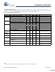
AC Analog Output Buffer Specifications
The following tables list guaranteed maximum and minimum specifications for the voltage and temperature ranges: 4.75V to 5.25V
and -40°C ≤ T
A
≤ 125°C. Typical parameters apply to 5V at 25°C and are for design guidance only.
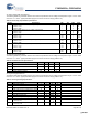
AC External Clock Specifications
The following tables list guaranteed maximum and minimum specifications for the voltage and temperature ranges: 4.75V to 5.25V
and -40°C ≤ T
A
≤ 125°C. Typical parameters apply to 5V at 25°C and are for design guidance only.
AC Programming Specifications
The following table lists guaranteed maximum and minimum specifications for the voltage and temperature ranges: 4.75V to 5.25V
and -40°C ≤ T
A
≤ 125°C. Typical parameters apply to 5V at 25°C and are for design guidance only.
Table 25. AC Analog Output Buffer Specifications
Symbol Description Min Typ Max Units
T
ROB
Rising Settling Time to 0.1%, 1V Step, 100 pF Load
Power = Low
Power = High
–
–
–
–
3
3
μs
μs
T
SOB
Falling Settling Time to 0.1%, 1V Step, 100 pF Load
Power = Low
Power = High
–
–
–
–
3
3
μs
μs
SR
ROB
Rising Slew Rate (20% to 80%), 1V Step, 100 pF Load
Power = Low
Power = High
0.6
0.6
–
–
–
–
V/μs
V/μs
SR
FOB
Falling Slew Rate (80% to 20%), 1V Step, 100 pF Load
Power = Low
Power = High
0.6
0.6
–
–
–
–
V/μs
V/μs
BW
OB
Small Signal Bandwidth, 20mV
pp
, 3dB BW, 100 pF Load
Power = Low
Power = High
0.8
0.8
–
–
–
–
MHz
MHz
BW
OB
Large Signal Bandwidth, 1V
pp
, 3dB BW, 100 pF Load
Power = Low
Power = High
300
300
–
–
–
–
kHz
kHz
Table 26. AC External Clock Specifications
Symbol Description Min Typ Max Units Notes
F
OSCEXT
Frequency 0.093 –24.24MHz
– High Period 20.6 – –ns
– Low Period 20.6
– –ns
– Power Up IMO to Switch 150
– – μs
Table 27. AC Programming Specifications
Symbol Description Min Typ Max Units Notes
T
RSCLK
Rise Time of SCLK 1 – 20 ns
T
FSCLK
Fall Time of SCLK 1 – 20 ns
T
SSCLK
Data Set up Time to Falling Edge of SCLK 40 – – ns
T
HSCLK
Data Hold Time from Falling Edge of SCLK 40 – – ns
F
SCLK
Frequency of SCLK 0 – 8 MHz
T
ERASEB
Flash Erase Time (Block) – 20 80
[9]
ms
T
WRITE
Flash Block Write Time – 80 320
[9]
ms
T
DSCLK
Data Out Delay from Falling Edge of SCLK – – 50 ns
T
PRGH
Total Flash Block Program Time (T
ERASEB
+ T
WRITE
), Hot
– – 200
[9]
ms T
J
≥ 0°C
T
PRGC
Total Flash Block Program Time (T
ERASEB
+ T
WRITE
), Cold
– – 400
[9]
ms T
J
< 0°C
[+] Feedback [+] Feedback