
User manual


CY8C24223A, CY8C24423A
Document Number: 38-12029 Rev. *H Page 20 of 34
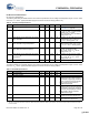
DC Analog PSoC Block Specifications
The following table lists guaranteed maximum and minimum specifications for the voltage and temperature ranges: 4.75V to 5.25V
and -40°C ≤ T
A
≤ 125°C. Typical parameters apply to 5V at 25°C and are for design guidance only.
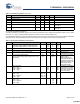
DC POR and LVD Specifications
The following table lists guaranteed maximum and minimum specifications for the voltage and temperature ranges: 4.75V to 5.25V
and -40°C ≤ T
A
≤ 125°C. Typical parameters apply to 5V at 25°C and are for design guidance only.
Note The bits PORLEV and VM in the following table refer to bits in the VLT_CR register. See the PSoC Technical Reference Manual
for more information on the VLT_CR register.
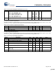
DC Programming Specifications
The following table lists guaranteed maximum and minimum specifications for the voltage and temperature ranges: 4.75V to 5.25V
and -40°C ≤ T
A
≤ 125°C. Typical parameters apply to 5V at 25°C and are for design guidance only.
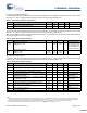
Table 17. DC Analog PSoC Block Specifications
Symbol Description Min Typ Max Units Notes
R
CT
Resistor Unit Value (Continuous Time) – 12.24 – kΩ
C
SC
Capacitor Unit Value (Switch Cap) – 80 – fF
Table 18. DC POR and LVD Specifications
Symbol Description Min Typ Max Units Notes
V
PPOR2
Vdd Value for PPOR Trip
PORLEV[1:0] = 10b – 4.55 4.70 V
Vdd must be greater
than or equal to 2.5V
during startup, reset
from the XRES pin, or
reset from watchdog.
V
LVD6
V
LVD7
Vdd Value for LVD Trip
VM[2:0] = 110b
VM[2:0] = 111b
4.62
4.710
4.73
4.814
4.83
4.950
V
V
Notes
9. For the full temperature range, the user must employ a temperature sensor user module (FlashTemp) or other temperature sensor, and feed the result to the
temperature argument before writing. Refer to the Flash APIs Application Note AN2015 at http://www.cypress.com under Application Notes for more information.
10. The maximum total number of allowed erase/write cycles is the minimum Flash
ENPB
value multiplied by the number of flash blocks in the device.
11. Flash data retention based on the use condition of ≤ 7000 hours at T
A
≤ 125°C and the remaining time at T
A
≤ 65°C.
Table 19. DC Programming Specifications
Symbol Description Min Typ Max Units Notes
Vdd
IWRITE
Supply Voltage for Flash Write Operations 4.75 – – V
I
DDP
Supply Current During Programming or Verify – 10 25 mA
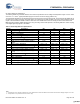
V
ILP
Input Low Voltage During Programming or Verify – – 0.8 V
V
IHP
Input High Voltage During Programming or Verify 2.1 – – V
I
ILP
Input Current when Applying V
ILP
to P1[0] or P1[1] During
Programming or Verify
– – 0.2 mA Driving internal pull
down resistor.
I
IHP
Input Current when Applying V
IHP
to P1[0] or P1[1] During
Programming or Verify
– – 1.5 mA Driving internal pull
down resistor.
V
OLV
Output Low Voltage During Programming or Verify – – 0.75 V
V
OHV
Output High Voltage During Programming or Verify 3.5 – Vdd V
Flash
ENPB
Flash Endurance (per block)
[9]
100 – – – Erase/write cycles per
block.
Flash
ENT
Flash Endurance (total)
[9, 10]
6,400 – – – Erase/write cycles.
Flash
DR
Flash Data Retention
[11]
15 – – Years
[+] Feedback [+] Feedback