
User manual


CY8C24223A, CY8C24423A
Document Number: 38-12029 Rev. *H Page 19 of 34
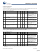
DC Analog Reference Specifications
The following tables list guaranteed maximum and minimum specifications for the voltage and temperature ranges: 4.75V to 5.25V
and -40°C ≤ T
A
≤ 125°C. Typical parameters apply to 5V at 25°C and are for design guidance only.
The guaranteed specifications are measured through the Analog Continuous Time PSoC blocks. The power levels for AGND refer to
the power of the Analog Continuous Time PSoC block. The power levels for RefHi and RefLo refer to the Analog Reference Control
register. The limits stated for AGND include the offset error of the AGND buffer local to the Analog Continuous Time PSoC block.
Note Avoid using P2[4] for digital signaling when using an analog resource that depends on the Analog Reference. Some coupling
of the digital signal may appear on the AGND.
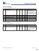
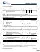
Table 16. DC Analog Reference Specifications
Symbol Description Min Typ Max Units
BG Bandgap Voltage Reference 1.25 1.30 1.35 V
– AGND = Vdd/2
[7]
Vdd/2 - 0.02 Vdd/2 Vdd/2 + 0.02 V
– AGND = 2 x BandGap
[7]
2.4 2.6 2.8 V
– AGND = P2[4] (P2[4] = Vdd/2)
[7]
P2[4] - 0.02 P2[4] P2[4] + 0.02 V
– AGND = BandGap
[7]
1.23 1.30 1.37 V
– AGND = 1.6 x BandGap
[7]
1.98 2.08 2.14 V
– AGND Column to Column Variation (AGND =
Vdd/2)
[7]
-0.035 0.000 0.035 V
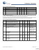
– RefHi = Vdd/2 + BandGap
[8]
Vdd/2 + 1.15 Vdd/2 +1.30 Vdd/2 +1.45 V
– RefHi = 3 x BandGap
[8]
3.65 3.9 4.15 V
– RefHi = 2 x BandGap + P2[6] (P2[6] = 1.3V)
[8]
P2[6] + 2.4 P2[6] + 2.6 P2[6] + 2.8 V
– RefHi = P2[4] + BandGap (P2[4] = Vdd/2)
[8]
P2[4] + 1.24 P2[4] +1.30 P2[4] + 1.36 V
– RefHi = P2[4] + P2[6] (P2[4] = Vdd/2, P2[6] =
1.3V)
[8]
P2[4] + P2[6] - 0.1 P2[4] + P2[6] P2[4] + P2[6] + 0.1 V
– RefHi = 3.2 x BandGap
[8]
3.9 4.16 4.42 V
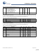
– RefLo = Vdd/2 – BandGap
[8]
Vdd/2 - 1.45 Vdd/2 - 1.3 1.15 V
– RefLo = BandGap
[8]
1.15 1.3 1.45 V
– RefLo = 2 x BandGap - P2[6] (P2[6] = 1.3V)
[8]
2.4 - P2[6] 2.6 - P2[6] 2.8 - P2[6] V
– RefLo = P2[4] – BandGap (P2[4] = Vdd/2)
[8]
P2[4] - 1.45 1.3 P2[4] - 1.15 V
– RefLo = P2[4]-P2[6] (P2[4] = Vdd/2, P2[6] = 1.3V)
[8]
P2[4] - P2[6] - 0.1 P2[4] - P2[6] P2[4] - P2[6] + 0.1 V
Notes
7. This specification is only valid when CT Block Power = High. AGND tolerance includes the offsets of the local buffer in the PSoC block. Bandgap voltage is 1.3V ± 0.05V.
8. This specification is only valid when Ref Control Power = High.
[+] Feedback [+] Feedback