
User manual


CY8C24223A, CY8C24423A
Document Number: 38-12029 Rev. *H Page 16 of 34
DC Electrical Characteristics
DC Chip-Level Specifications
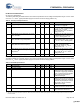
The following table lists guaranteed maximum and minimum specifications for the voltage and temperature ranges: 4.75V to 5.25V
and -40°C ≤ T
A
≤ 125°C. Typical parameters apply to 5V at 25°C and are for design guidance only.
DC General Purpose I/O Specifications
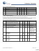
The following tables list guaranteed maximum and minimum specifications for the voltage and temperature ranges: 4.75V to 5.25V
and -40°C ≤ T
A
≤ 125°C. Typical parameters apply to 5V at 25°C and are for design guidance.
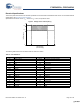
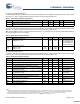
Table 11. DC Chip-Level Specifications
Symbol Description Min Typ Max Units Notes
Vdd Supply Voltage 4.75 – 5.25 V See table titled DC POR and LVD
Specifications on page 20
I
DD
Supply Current – 5 8 mA Conditions are Vdd = 5.25V, -40
o
C ≤
T
A
≤ 125
o
C, CPU = 3 MHz, 48 MHz
disabled, VC1 = 1.5 MHz,
VC2 = 93.75 kHz, VC3 = 93.75 kHz,
Analog power = off.
I
SB
Sleep (Mode) Current with POR, LVD, Sleep
Timer, and WDT.
[6]
– 4 13 μA Conditions are with internal low speed
oscillator active, Vdd = 5.25V, -40
o
C ≤
T
A
≤ 55
o
C. Analog power = off.
I
SBH
Sleep (Mode) Current with POR, LVD, Sleep
Timer, and WDT at high temperature.
[6]
– 4 100 μA Conditions are with internal slow
speed oscillator active, Vdd = 5.25V,
55
o
C < T
A
≤ 125
o
C. Analog power =
off.
I
SBXTL
Sleep (Mode) Current with POR, LVD, Sleep
Timer, WDT, and external crystal.
[6]
– 6 15 μA Conditions are with properly loaded, 1
μW max, 32.768 kHz crystal.
Vdd = 5.25V, -40
o
C ≤ T
A
≤ 55
o
C.
Analog power = off.
I
SBXTLH
Sleep (Mode) Current with POR, LVD, Sleep
Timer, WDT, and external crystal at high
temperature.
[6]
– 6 100 μA Conditions are with properly loaded,
1μW max, 32.768 kHz crystal.
Vdd = 5.25V, 55
o
C < T
A
≤ 125
o
C.
Analog power = off.
V
REF
Reference Voltage (Bandgap) 1.25 1.3 1.35 V Trimmed for appropriate Vdd.
Note
6. Standby current includes all functions (POR, LVD, WDT, Sleep Timer) needed for reliable system operation. This must be compared with devices that have similar
functions enabled.
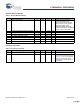
Table 12. DC GPIO Specifications
Symbol Description Min Typ Max Units Notes
R
PU
Pull up Resistor 4 5.6 8 kΩ
R
PD
Pull down Resistor 4 5.6 8 kΩ
V
OH
High Output Level 3.5 – – V IOH = 10 mA, Vdd = 4.75 to 5.25V
(maximum 40 mA on even port pins
(for example, P0[2], P1[4]), maximum
40 mA on odd port pins (for example,
P0[3], P1[5])). 80 mA maximum
combined IOH budget.
V
OL
Low Output Level – – 0.75 V IOL = 25 mA, Vdd = 4.75 to 5.25V
(maximum 100 mA on even port pins
(for example, P0[2], P1[4]), maximum
100 mA on odd port pins (for example,
P0[3], P1[5])). 150 mA maximum
combined IOL budget.
I
OH
High Level Source Current 10 – – mA V
OH
≥ Vdd-1.0V, see the limitations of
the total current in the note for V
OH.
I
OL
Low Level Sink Current 25 – – mA V
OL
≤ 0.75V, see the limitations of the
total current in the note for V
OL.
[+] Feedback [+] Feedback