
Specifications


October 25, 2006 Cypress Semiconductor – Rev. ** 7
LIN Bus 2.0 Reference Design 1. LIN Bus 2.0 Kit
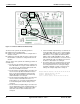
Figure 1-2. Layout of Node-Specific Switches and LEDs
Periodically, the master node sends its switch state informa-
tion to slave 1 and then polls both slaves for their switch
state information. In response, the master and slaves dis-
play the state of the information as specified by the switch-
to-display relationship. Figure 1-3 and the following list show
the switches and the LEDs that they control:
■ Master node dip-switches 8 to 1 control slave 1’s LEDs 1
to 8. Note that the dip-switch numbering is reversed but
is oriented such that the left most switch, numbered 8,
controls the left most LED of slave 1.
■ Slave 1’s dip-switches 8 to 5 control master node LEDs
1 to 4.
■ Slave 1 measures the resistance connected between
P0[1] and P0[3] and sends this information to the master.
To make the resistance measurement, a reference resis-
tance of 2.2K is connected between P0[1] and P0[2].
These resistance connections can be made to the
header (SV3) meant for port 0 of slave 1.
■ Slave 1’s dip-switches 2 and 1 control slave 2 LEDs, D2
and D4. These switches are configured to implement a
left / right turn indicator. When one of these switches is
closed, D2 or D4 blinks.
■ Slave 2’s push-button switches, S2 and S1, control mas-
ter node LEDs 5 and 6.
■ The remaining switches and LEDs are not used, but
board connections are provided for use in the prototype
area.
SW2
S2
SW1
D2
U7
U8
D4
S1