
Specifications


1. LIN Bus 2.0 Kit LIN Bus 2.0 Reference Design
6 Cypress Semiconductor – Rev. ** October 25, 2006
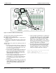
Figure 1-1. LIN Bus Demonstration Board
The master node and slave 1 are both implemented in a 28-
pin part, CY8C27443-24PXI. Slave 2 is implemented in an
8-pin part, CY8C27143-24PXI.
The CD-ROM that is included with this kit has all project files
for the designed-in devices as well as project files for auto-
motive grade devices.
1.4 LIN Bus Demonstration
The LIN bus demonstration board is divided into four
regions: master node, slave 1, slave 2, and the prototype
area.
The master node has a bank of 8 dip-switches, SW2, and a
bank of 10 LEDs, U8. Slave 1 also has a set of 8 dip-
switches, SW1, and a bank of 10 LEDs, U7. Slave 2 has 2
push-button switches, S1 and S2, and 2 individual green
LEDs, D2 and D4. Figure 1-1 shows the positions of these
components.
Master
Node
Slave
1
Slave
2
Prototype
Area
Power
Supply
Power
Jack
Master
Serial Port