
Specifications


3. Master Design IP LIN Bus 2.0 Reference Design
28 Cypress Semiconductor – Rev. ** October 25, 2006
actually send the command, point the l_sch_set function to
a master request frame and call the l_sch_tick function.
ld_read_by_id
C Prototype: void ld_read_by_id(l_u8 NAD, l_u16
supplier_id, l_u16 function_id, l_u8 id,
char* data);
Description: This call requests the node with the NAD to
return the property associated with the ID parameter. When
the next call to ld_is_ready returns true, the RAM area spec-
ified by data contains between one and five bytes of data
according to the request.
Parameters:
NAD: The NAD of the node.
supplier_id: The supplier_id of the slave.
function_id: The function ID of the slave.
id: Indicates the property to read.
data: Pointer to the RAM buffer where the slave response is
deposited.
Returns: None.
Usage Notes: When this function is called, the diagnostic
buffer in the RAM is updated with all the parameters. To
actually send the command, point the l_sch_set function to
a master request frame and call l_sch_tick function. Then
follow the master request frame with a slave response frame
to get the slave’s response.
ld_conditional_change_nad
C Prototype: void
ld_conditional_change_NAD(l_u8 NAD, l_u8 id,
l_u8 byte, l_u8 mask, l_u8 invert, l_u8
new_NAD);
Description: This call changes the NAD if the node proper-
ties fulfill the test specified by id, byte, mask and invert. For
details, refer to the LIN Diagnostics Specification in the LIN
2.0 protocol document.
Parameters:
NAD: The NAD of the node.
Id, byte, mask, invert: Test conditions.
new_NAD: The new NAD to assign to the slave.
Returns: None.
Usage Notes: When this function is called, the diagnostic
buffer in the RAM is updated with all the parameters. To
actually send the call, point the l_sch_set function to a mas-
ter request frame and call the l_sch_tick function.
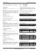
3.8 Time Study
3.8.1 ISR Timing
The following tables list the time taken by some of the impor-
tant branches of the ISR in the LIN master node. The CPU
overhead for various conditions are roughly computed using
these tables.
Note that the times indicated are approximate and may
change during future revisions of the firmware
.
Table 3-5. Synchro Break Interrupt
Sl. No. Stage No. Of Cycles
Time(µS)
1 Break field sent 864 36.00
Table 3-6. Synchro Break Bit Time Interrupt
Sl. No. Stage No. Of Cycles
Time(µS)
1 Once every bit time for 14 bits 63 2.63
Table 3-7. TX Interrupt
Sl. No. Stage No. Of Cycles
Time(µS)
1 When a data byte is sent 58 2.42
Table 3-8. TX Bit Time Interrupt
Sl. No. Stage No. Of Cycles
Time(µS)
1 Once every bit time 65 2.71
2 When all bytes have been transmit-
ted
989 41.21
Table 3-9. RX Interrupt
Sl. No. Stage No. Of Cycles
Time(µS)
1 Data byte received 95 3.96
2 Frame reception complete, normal 1679 69.96
3 Frame reception complete, slave
response
1776 74.00
Table 3-10. RX Bit Time Interrupt
Sl. No. Stage No. Of Cycles
Time(µS)
1 Once in 5 bit times, normal 27 1.13
2 Once in 5 bit times, slave not
responding
970 40.42