
Specifications


LIN Bus 2.0 Reference Design 1
Contents
1.1 LIN Bus 2.0 Demonstration Kit Description .......................................................................................5
1.1.1 Introduction ..............................................................................................................5
1.2 Kit Contents ...............................................................................................................................5
1.3 Getting Started...........................................................................................................................5
1.4 LIN Bus Demonstration..............................................................................................................6
1.5 Master Node Port Pin Usage .....................................................................................................9
1.6 Slave 1 Port Pin Usage..............................................................................................................9
1.7 Slave 2 Port Pin Usage............................................................................................................10
1.8 Design IP .................................................................................................................................10
1.9 Demonstration Projects............................................................................................................10
1.10 Other Features.........................................................................................................................10
1.11 Support ....................................................................................................................................10
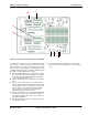
2.1 System Architecture Overview ..........................................................................................................11
2.2 Features of the PSoC LIN Bus 2.0 Design...............................................................................11
2.3 LIN Frame ................................................................................................................................11
2.3.1 Basic LIN Frame ...................................................................................................11
2.3.2 Break Field.............................................................................................................12
2.3.3 Synch Byte.............................................................................................................12
2.3.4 Protected Identifier.................................................................................................12
2.3.5 Data .......................................................................................................................12
2.3.6 Checksum..............................................................................................................12
2.3.7 Frame Transfers on the LIN Bus............................................................................12
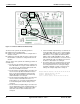
2.4 Hardware Architecture .............................................................................................................13
2.4.1 LIN Transceiver .....................................................................................................13
2.4.2 Voltage Regulator .................................................................................................13
2.4.3 External Pin Connections ......................................................................................13
3.1 Master Software Architecture ............................................................................................................15
3.1.1 Overview................................................................................................................15
3.1.2 Foreground Processing..........................................................................................15
3.1.3 Timing and Interrupts .............................................................................................16
3.2 Device Configurations..............................................................................................................16
3.2.1 Synchro Break Configuration.................................................................................16
3.2.2 Data Transmission Configuration...........................................................................16
3.2.3 Data Reception Configuration................................................................................16
3.3 Firmware ..................................................................................................................................17
3.3.1 Overview................................................................................................................17
3.3.2 Synchro Break Interrupt.........................................................................................17
3.3.3 TX Interrupt............................................................................................................17
3.3.4 RX Interrupt............................................................................................................17
3.3.5 Bit Time Interrupt ...................................................................................................17
3.3.5.1 Synchro Break Configuration ..............................................................17
3.3.5.2 Data Transmission Configuration .......................................................17
3.3.5.3 Data Reception Configuration .............................................................18