
Specifications


October 25, 2006 Cypress Semiconductor – Rev. ** 19
LIN Bus 2.0 Reference Design 3. Master Design IP
7. The “Resolve name conflicts” window lists functions in
the imported design that have the same name as func-
tions in the existing project. When there is a name con-
flict, clicking the “Auto Resolve” button automatically
renames the conflicting function names.
8. Below this, details of the design such as date of creation,
description and the base part number are displayed.
9. Click OK.
10. Now in the Device Selection window, select the device
for the project.
11. Select “Generate main file using C.”
12. Select “Device Editor” as the Designer State.
13. Click Finish.
14. A Design Import Status window opens and displays the
import status.
15. When the design is imported, PSoC Designer opens the
Device Editor.
16. Four configurations are visible. The base configuration
with the project name, the Synchro Break Configuration,
Data Transmission Configuration and the Data Recep-
tion Configuration.
17. Go to Project >> Settings, Device Editor tab. In the con-
figuration initialization type, select “Direct Write (Speed
Efficient).”
18. Now switch to the base configuration and select all the
user modules to include in the main application.
3.6.2 Configuring Global Resources
Now switch to the Interconnect View and select the base
configuration. First, configure all the global resources
related to the LIN design. Whatever changes made to the
base configuration, are reflected in the other three loadable
configurations.
1. Set CPU speed to 24 MHz. (Set the CPU speed to 12
MHz for the CY8C27x43 automotive grade device.)
2. Set 32 kHz to External.
3. Set the PLL to Enabled.
4. Set VC1 divider to 12.
These are the required global resources for the LIN master.
The clock VC1 is used as the source clock to LIN modules.
The divider is set to 12 in the firmware so that the output of
VC1 is 2 MHz. Take this into account when using VC1 and
VC2 in the main application. You can set all the other global
resources in your main application.
3.6.3 Configuring GPIO
Next, decide the TX and RX pins of the LIN bus. To properly
select their drive modes in all configurations, follow these
steps carefully.
1. Switch to the base configuration. Use the Config >>
Restore default pinout. All the pins in the GPIO configu-
ration pane become StdCPU, High Z Analog, DisableInt.
Repeat this step for the synchro break, data transmis-
sion and data reception configurations.
2. Return to the base configuration.
3. In the GPIO configuration pane, rename the port pin you
plan to use as the RX pin to “RX.” Then rename the pin
you plan to use as the TX pin as “TX.” Capitalize these
letters.
4. In the Select column of the RX pin, select the
GlobalInOdd_x or GlobalInEven_x. The drive mode
automatically becomes High Z.
5. In the Select column of the TX pin, select the
GlobalOutOdd_x or GlobalOutEven_x. The drive mode
automatically becomes Strong.
6. Switch to synchro break, data transmission and data
reception configurations and check that these changes
are reflected.
The GPIO configuration is done. After this, modify the GPIO
of the other port pins according to the main project require-
ments. Whenever a modification is done in the base configu-
ration, the same settings are updated in the other three
configurations. Thus, regardless of which configuration is
active, the GPIO state of the main application is maintained.
When the process is complete, the configuration of the TX
and RX pins looks like this:
3.6.4 Routing the Signals
The next step is to route the signals to the digital blocks of
the LIN configurations.
1. Go to the Synchro Break Configuration.
2. Route the Compare Out of the synchro break counter to
the appropriate Row_1_Output_x line. For example, if
you have configured P0[3] as TX pin, then route the
Compare out to Row_1_Output_3 net.
3. From this Row_1_Output_x net, route the signal to the
appropriate GlobalOut bus to which the TX pin is con-
nected.
4. Switch to the Data Transmission Configuration.
5. Route the output of the TX8 to the same
Row_1_Output_x line used by the synchro break
counter (step 2) and from there to the GlobalOut bus to
which TX pin is connected.
6. Switch to the Data Reception Configuration.
7. Route the Global_Input net to which RX is connected, to
an appropriate Row_1_Input_x net. Select Synch to
SysClk in the Synchronization box. For example, if P0[2]
is used as RX, then connect GlobalIn_Even_2 bus to
Row_1_Input_2 net.
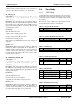
Table 3-1. TX Pin
Configuration Name Port Select Drive Interrupt
Base TX As selected GlobalOut Strong DisableInt
Synchro Break TX As selected GlobalOut Strong DisableInt
Data Transmission TX As selected GlobalOut Strong DisableInt
Data Reception TX As selected GlobalOut Strong DisableInt
Table 3-2. RX Pin
Configuration Name Port Select Drive Interrupt
Base RX As selected GlobalIn High Z DisableInt
Synchro Break RX As selected GlobalIn High Z DisableInt
Data Transmission RX As selected GlobalIn High Z DisableInt
Data Reception RX As selected GlobalIn High Z DisableInt