
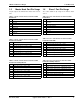
Specifications


3. Master Design IP LIN Bus 2.0 Reference Design
16 Cypress Semiconductor – Rev. ** October 25, 2006
3.1.3 Timing and Interrupts
Automotive applications are often real-time driven. As a
result, the LIN driver only uses interrupts with no active loop
or blocking functions. Overhead measurements made on a
LIN bus with messages transferred at 19200 bauds and the
PSoC CPU running at 24 MHz, show a 0% overhead
between messages, and a maximum of 5% overhead while
sending or receiving messages. Refer to Time Study on
page 28 in this chapter.
3.2 Device Configurations
The LIN master design uses dynamic reconfiguration and
has three configurations, the Synchro Break Configuration,
Data Transmission Configuration and the Data Reception
Configuration. The Synchro Break Configuration generates
the break field. The Data Transmission Configuration sends
the synchronization byte and any data bytes to be transmit-
ted followed by the checksum byte. The Data Reception
Configuration receives the slave’s response data.
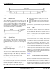
3.2.1 Synchro Break Configuration
Figure 3-1 shows the module placement for the Synchro
Break Configuration. This configuration has one 8-bit
counter (SB_Baud_Rate_Counter) that generates the baud
clock. The output frequency of this clock generator is eight
times the baud rate. There is a second 8-bit counter
(SB_Bit_time_counter) that is used to generate an interrupt
every bit time. Finally, there is a third 8-bit counter
(Synchro_Break_Counter) that generates the actual break
field. The period and compare values of
Synchro_Break_Counter are set in such a way that one full
cycle of the counter produces a break time approximately
equal to 13 bit times and the break delimiter equal to one bit
time. The TX and RX pins are compared to detect any bit
error inside the Bit_time_counter ISR.
Figure 3-1. Synchro Break Configuration
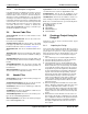
3.2.2 Data Transmission Configuration
Figure 3-2 shows the user module placement for the Data
Transmission Configuration. This configuration has one 8-bit
counter that generates the baud rate
(DT_Baud_rate_counter), one 8-bit counter that is used to
generate interrupts every bit time for detecting bit errors
(DT_Bit_time_counter), and one TX8 User Module to trans-
mit data (TX8). The baud rate generator is configured to
generate a clock eight times that of the baud clock and feed
the TX8 block’s clock input. When break field generation is
complete, the Data Transmission Configuration is loaded
and 0x55 is transmitted as the synch byte. Next, the pro-
tected identifier is transmitted. The protected identifier is fol-
lowed by master’s data and the checksum if the frame is
MASTER_TO_SLAVE. Also during the data transmission,
the Bit_time_counter generates an interrupt every bit time.
Inside the Bit_time_counter’s ISR, the TX and RX pins are
compared. If they are not equal, then the BIT_ERROR flag
is set and transmission of the current frame is aborted.
Figure 3-2. Data Transmission Configuration
3.2.3 Data Reception Configuration
Figure 3-3 shows the user module placement for the Data
Reception Configuration. This has one 8-bit counter that
generates the baud rate (DR_Baud_rate_counter), one 8-bit
counter that is used to generate interrupts every five bit
times for detecting the slave non-response timeout
(DR_Bit_time_counter), and one RX8 User Module that
receives data (RX8). The DR_Baud_rate_counter is config-
ured to generate a clock eight times that of the baud clock
and feed the RX8 block’s clock input. The received bytes
are transferred to the temporary buffer inside the RX8 ISR.
When all the bytes indicated by the variable bNbDataToRe-
ceive have been received, the master processes the
received data. Also, the bit time counter generates an inter-
rupt every five bit times and a timeout counter is decre-
mented inside the DT_Bit_time_counter ISR. The timeout is
set as number of bit times according to the length of the
frame. If the frame is not completed within this timeout (if the
concerned slave stops transmitting), the Synchro Break
Configuration is loaded and the “Slave Not Responding”
error flag is set.
Figure 3-3. Data Reception Configuration