
Specifications


October 25, 2006 Cypress Semiconductor – Rev. ** 13
LIN Bus 2.0 Reference Design 2. System Architecture
frames in the Schedule table have been transmitted, the
next cycle starts again from the first frame of the table.
The LIN 2.0 API has many functions to manage the Sched-
ule table. It has functions to select tables, to initiate the
transfer of the next frame in the current table, and so on.
More details on these APIs are found in section 3, Master
Design APIs, on page 25.
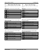
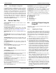
Figure 2-5. Hardware Configuration of a LIN Master/Slave
2.4 Hardware Architecture
Figure 2-5 shows the hardware architecture for the LIN Mas-
ter/Slave.
2.4.1 LIN Transceiver
Because the physical LIN bus is held at Vbat in the range of
8 to 18 volts, a LIN transceiver device is required to connect
the LIN bus with the PSoC chip. The LIN transceiver con-
verts the single wire LIN bus at 8V – 18 volts to TTL-level TX
and RX signals, which can be connected to the PSoC.
2.4.2 Voltage Regulator
You must use a voltage regulator to provide the PSoC Vcc
supply. LIN transceivers with built-in regulators are avail-
able.
2.4.3 External Pin Connections
You have the option to decide which pins to use for the TX
and RX pins in the design. These connections are done in
the Device Editor of PSoC Designer. Details on how to con-
figure the pins are in section 5, Using the Design IP, on
page 35.