
Specifications


1. LIN Bus 2.0 Kit LIN Bus 2.0 Reference Design
10 Cypress Semiconductor – Rev. ** October 25, 2006
1.7 Slave 2 Port Pin Usage
The section details the pin usage for the LIN bus PSoC
slave 2:
1.8 Design IP
LIN Master Node and LIN Slave Node Design IP are pro-
vided on the CD and on the Cypress Semiconductor web
site at http://www.cypress.com.
Design IP in PSoC Designer allows a user to import the
required solution, precomposed of configurations and soft-
ware APIs, to quickly and easily implement a LIN bus node.
To import the Design IP into a project, use the PSoC
Designer Design Browser (under C
onfig >> Import Design).
The LIN Master Node Design IP and the LIN Slave Node
Design IP documentation are located in the root directory of
the CD.
1.9 Demonstration Projects
Also included on the CD are the three PSoC projects that
implement the master and slave nodes on the demonstra-
tion board delivered with this design kit. The demonstration
projects are in the following directories of the CD:
■ Demonstration Projects\Master Node\MasterLinDemo
■ Demonstration Projects\Slave 1 Node\CLinSlaveDemo
■ Demonstration Projects\Slave 2 Node\CLinSlaveDemo2
1.10 Other Features
In addition to the three LIN nodes, the demonstration board
provides several other features:
■ Unregulated 12V DC 500 mA power supply for prototype
use.
■ Regulated 5V DC 500 mA power supply for prototype
use.
■ U12 header provides access to LIN bus for probing or
bus extension.
■ Disconnectable LIN nodes from the LIN bus by removing
the JP1, JP2, or JP3 jumpers.
■ Prototype area provides power and ground connections,
and two strips of holes for prototyping. The holes are
connected in rows of three to simplify connections, and if
required, the traces can be cut.
Figure 1-4. Prototype Area Through Hole Connections
■ Install header U13 to short LED D2. This allows develop-
ment of self-diagnostic indicator faults.
■ Remove jumper JP4 to provide an open circuit at LED
D4. This provides an additional way to develop self-diag-
nostic indicator faults.
■ You can emulate master node and slave 1 using a uni-
versal emulation pod, from a PSoC Basic Development
Kit, mounted on the standard 28-pin DIP foot.
■ You can emulate slave 2 using a universal emulation
pod mounted on the standard 8-pin DIP foot.
■ The four unused LEDs in the master node LED array are
provided on pads LED 0-3 for prototyping.
■ The two unused LEDs in the slave 1 LED array are pro-
vided on pads LED 4-5 for prototyping.
1.11 Support
Support for the PSoC device, the development tools or the
LIN bus demonstration board can be found on our web site
at http://www.cypress.com, http://www.cypress.com/support
or by calling the Applications Hotline at 425.787.4814.
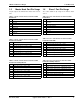
Table 1-7. Port 0 – Pins
2 Push button controls master, Port1_3 LED
4 LIN bus TX
5 LIN bus RX
7 Push button controls master, Port1_2 LED
Table 1-8. Port 1 – Pins
0 Blinking LED controlled by slave 1, Port2_3 switch
1 Blinking LED controlled by slave 1, Port2_2 switch
5V
Gnd
Gnd
5V