PSoC CY8C20x34 TRM PSoC® CY8C29x66, CY8C27x43, CY8C27x43E, CY8C21x34 LIN Bus 2.0 PSoC Reference Design. Revision ** Cypress Semiconductor 198 Champion Court San Jose, CA 95134-1709 Phone (USA): 800.858.1810 Phone (Intnl.): 408.943.2600 http://www.cypress.
Copyrights Copyrights Copyright © 2006 Cypress Semiconductor Corporation. All rights reserved. Cypress, the Cypress logo, and PSoC® are registered trademarks and PSoC Designer™, Programmable System-on-Chip™, and PSoC Express™ are trademarks of Cypress Semiconductor Corporation (Cypress). All other trademarks or registered trademarks referenced herein are the property of their respective owners.
Contents 1.1 LIN Bus 2.0 Demonstration Kit Description .......................................................................................5 1.1.1 Introduction ..............................................................................................................5 1.2 Kit Contents ...............................................................................................................................5 1.3 Getting Started ......................................................................
Contents 3.4 3.5 3.6 Source Code Files ................................................................................................................... 18 Header Files ............................................................................................................................ 18 Creating a Project Using the Design IP ................................................................................... 18 3.6.1 Importing the Design ..........................................................
Contents 4.6.5.1 RAM Allocation ....................................................................................36 Frame Definition.....................................................................................................37 Response_Error Bit Definition................................................................................37 Node Information ...................................................................................................37 Adding the Main Application .............
Contents 4 LIN Bus 2.
1. LIN Bus 2.0 Kit 1.1 LIN Bus 2.0 Demonstration Kit Description 1.1.1 Introduction The LIN Bus Demonstration Kit demonstrates the ability of the PSoC® Programmable System-on-Chip™ to implement LIN bus, Local Interconnect Network, standard protocol. The LIN bus was developed to fill the need for a low cost automotive network to complement existing networks. LIN bus also finds many uses in non-automotive distributed systems where a robust, low-speed and low-cost protocol is required.
1. LIN Bus 2.0 Kit LIN Bus 2.0 Reference Design Power Jack Power Supply Master Serial Port Master Node Slave 1 Prototype Area Slave 2 Figure 1-1. LIN Bus Demonstration Board The master node and slave 1 are both implemented in a 28pin part, CY8C27443-24PXI. Slave 2 is implemented in an 8-pin part, CY8C27143-24PXI. The CD-ROM that is included with this kit has all project files for the designed-in devices as well as project files for automotive grade devices. 1.
LIN Bus 2.0 Reference Design 1. LIN Bus 2.0 Kit U8 SW2 U7 SW1 S2 S1 D2 D4 Figure 1-2. Layout of Node-Specific Switches and LEDs Periodically, the master node sends its switch state information to slave 1 and then polls both slaves for their switch state information. In response, the master and slaves display the state of the information as specified by the switchto-display relationship.
1. LIN Bus 2.0 Kit LIN Bus 2.0 Reference Design Figure 1-3. Switch-to-LED Control Relationship The master node performs the following operations. ■ Initializes the LIN communication. ■ Calls the node configuration function to configure slave 1 and slave 2 nodes. ■ Initializes the Schedule table. The frame sequence and time allotted for each frame is configured in the Schedule table.
LIN Bus 2.0 Reference Design 1.5 1. LIN Bus 2.0 Kit Master Node Port Pin Usage 1.6 Slave 1 Port Pin Usage The pin usage for the LIN bus PSoC master node is as follows: The section details the pin usage for the LIN bus PSoC slave 1: Table 1-1. Port 0 – Pins Connect to User-Accessible Header Row Table 1-4.
1. LIN Bus 2.0 Kit 1.7 LIN Bus 2.0 Reference Design Slave 2 Port Pin Usage The section details the pin usage for the LIN bus PSoC slave 2: Table 1-7. Port 0 – Pins 2 Push button controls master, Port1_3 LED 4 LIN bus TX 5 LIN bus RX 7 Push button controls master, Port1_2 LED Table 1-8. Port 1 – Pins 0 Blinking LED controlled by slave 1, Port2_3 switch 1 Blinking LED controlled by slave 1, Port2_2 switch 1.8 1.
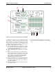
2. System Architecture 2.1 Overview The LIN bus, Local Interconnect Network, is an asynchronous, 1 wire, single master, multiple slave network. It is most commonly used in automobile networks. ■ ■ ■ 2.2 ■ ■ ■ ■ ■ ■ ■ Features of the PSoC LIN Bus 2.0 Design Single master, multiple slaves - up to 16 slaves. Message-based protocol. Single wire - maximum 40 m. Data rates of 2.4K, 4.8K, 9.6K and 19.2K are supported by master. Slaves capable of synchronizing to any baud rate from 2K to 20K.
2. System Architecture LIN Bus 2.0 Reference Design Figure 2-2. Structure of a Byte Field 2.3.2 Break Field ■ The break symbol is used to signal the beginning of a new frame. It is the only field that does not comply with Figure 22. A break is always generated by the master and is at least 13 bits of dominant value, including the start bit, followed by a break delimiter, as shown in Figure 2-3. The break delimiter is at least one nominal bit-time long.
LIN Bus 2.0 Reference Design 2. System Architecture frames in the Schedule table have been transmitted, the next cycle starts again from the first frame of the table. The LIN 2.0 API has many functions to manage the Schedule table. It has functions to select tables, to initiate the transfer of the next frame in the current table, and so on. More details on these APIs are found in section 3, Master Design APIs, on page 25. Figure 2-5. Hardware Configuration of a LIN Master/Slave 2.
2. System Architecture 14 LIN Bus 2.0 Reference Design Cypress Semiconductor – Rev.
3. Master Design IP 3.1 Software Architecture 3.1.1 Overview The software architecture maximizes interrupt processing to minimize the processing overhead on the end application. All message processing through configurations is performed at the interrupt level. Each stage is designed as a state machine and, upon completion, this state machine unloads itself and loads in the next required configuration to propagate the message to completion through the LIN message protocol sequence.
3. Master Design IP 3.1.3 LIN Bus 2.0 Reference Design Timing and Interrupts Automotive applications are often real-time driven. As a result, the LIN driver only uses interrupts with no active loop or blocking functions. Overhead measurements made on a LIN bus with messages transferred at 19200 bauds and the PSoC CPU running at 24 MHz, show a 0% overhead between messages, and a maximum of 5% overhead while sending or receiving messages. Refer to Time Study on page 28 in this chapter. 3.
LIN Bus 2.0 Reference Design 3.3 3.3.1 3. Master Design IP Firmware 3.3.4 Overview The initiation of a frame is done by the l_sch_tick function. This function first reads the Schedule table and loads the frame parameters of the frame to transmit. It then loads the Synchro Break Configuration and starts the synchro break timer. This timer is configured to generate a dominant state of 13 bit times and a recessive (logic high level on the bus) state of one bit time.
3. Master Design IP 3.3.5.3 LIN Bus 2.0 Reference Design Data Reception Configuration In the Data Reception Configuration, the bit time counter is configured to generate an interrupt every five bit times. Inside this ISR, a timeout counter is decremented by five. This timeout counter is initialized by the l_sch_tick function according to the number of data present in the frame. In a normal frame transaction, the frame is completed before this counter becomes zero.
LIN Bus 2.0 Reference Design 3. Master Design IP 7. The “Resolve name conflicts” window lists functions in the imported design that have the same name as functions in the existing project. When there is a name conflict, clicking the “Auto Resolve” button automatically renames the conflicting function names. 8. Below this, details of the design such as date of creation, description and the base part number are displayed. 9. Click OK. 10.
3. Master Design IP LIN Bus 2.0 Reference Design 8. Select Row_1_Input_x (step 7) as the input to the RX8 User Module. 9. Switch to the base configuration. 10. Make the connection from Row_1_Output_x net to the Global bus as used by the Data Transmission and Synchro Break configurations in the base configuration. 11. Make the connection from Global_In bus to the Row_1_Input_x net as used by the Data Reception Configuration. With this routing of signals, the hardware configuration is complete. 3.6.
LIN Bus 2.0 Reference Design 3. Master Design IP A. Checksum Type: This entry defines the checksum type used for the particular frame. There are two types of checksums, CSUM_CLASSIC and CSUM_EXTENDED. CSUM_CLASSIC is used for frames that belong to LIN slaves of version 1.3 or less and for diagnostic frames. CSUM_EXTENDED is used for LIN 2.0 slaves. B. Data Count: This entry indicates the length of data carried by the frame. For LIN1.x slaves, this parameter is left as zero.
3. Master Design IP LIN Bus 2.0 Reference Design _MasterRequest: MasterRequest: db CSUM_CLASSIC ; Checksum Type db 8 ; Data count db abDiagBuffer ; Buffer address they are in the RAM. The following are the entries in the SignalTable.h file.
LIN Bus 2.0 Reference Design 3.6.11.2 3. Master Design IP An Example Schedule Table Here is an example Schedule table. The name of the table is Schedule1. This table has Frame1, Frame2, Frame3 and Frame4 (which are defined in the SignalTable.asm file) in the order they are entered in the Schedule table. Schedule table example: _Schedule1: Schedule1: dw Frame1, 20 dw Frame3, 10 dw Frame2, 10 dw Frame4, 10 dw 0xFFFF The last entry in the Schedule table is the table terminator.
3. Master Design IP LIN Bus 2.0 Reference Design from this function. If the dominant state is less than 250 µS or if the state does not become recessive for more than 5 ms, the processor is put to sleep again. The processor can be configured to wake up on some other interrupt if the master must wake up on its own to complete some other task. For example, if the master must wake up upon a sleep interrupt and perform some operation, add code for this also inside the function.
LIN Bus 2.0 Reference Design 3. Master Design IP // Code to update the Frame5 buffer with the signal l_sporadic_frame_queue |= 0x04; } Description: The l_sch_tick function follows a schedule. When called, it initiates the next due frame in the current Schedule table. When the end of the current table is reached, the function starts from the beginning of the schedule. Only the bits corresponding to the frames in the Sporadic Frame table are set by the main function. Parameters: None. 3.
3. Master Design IP LIN Bus 2.0 Reference Design Example: For example, to write two bytes to Frame1 from the first byte of the buffer from another buffer called TempBuffer, use this code: l_bytes_wr(Frame1, 0, 2, TempBuffer); Parameters: None. Returns: None. Note that the first byte of the frame buffer has an offset of zero. That is why zero was used as the offset parameter. l_ifc_goto_sleep Returns: None. Description: This function generates the go to sleep command on the LIN bus.
LIN Bus 2.0 Reference Design 3. Master Design IP Description: Clears the LIN ready flag. Parameters: None. Table 3-4. Returns: None. Flag LinMaster_SetReadyFlag C Prototype: (void); void LinMaster_ClrReadyFlag Description: Sets the LIN ready flag. This function is called inside the schedule timer’s ISR when a frame slot is complete. Parameters: None. Returns: None. 3.7.3 LIN Node Configuration API Functions Description LD_SUCCESS The call succeeded. LD_NEGATIVE The call failed.
3. Master Design IP LIN Bus 2.0 Reference Design actually send the command, point the l_sch_set function to a master request frame and call the l_sch_tick function. 3.8 3.8.1 ld_read_by_id C Prototype: void ld_read_by_id(l_u8 NAD, l_u16 supplier_id, l_u16 function_id, l_u8 id, char* data); Description: This call requests the node with the NAD to return the property associated with the ID parameter.
LIN Bus 2.0 Reference Design 3. Master Design IP The overall CPU overhead for a frame is calculated by adding all the time components for a frame and then finding the fraction of the total frame time. Remember, this method only gives the overhead over a complete frame. The overhead at different instances of the frame may be different. 3.8.2 Calculation of CPU Overhead Over a Frame The following calculations are based on a baud rate of 19.2 kbps and CPU speed of 24 MHz.
3. Master Design IP 30 LIN Bus 2.0 Reference Design Cypress Semiconductor – Rev.
4. Slave Design IP 4.1 Software Architecture 4.1.1 Overview The software architecture maximizes interrupt processing to minimize the processing overhead on the end application. All processing of the current message using the configurations is performed at the interrupt level. Each stage is designed as a state machine and at completion, unloads itself and loads in the next required configuration to propagate the message to completion via LIN message protocol sequence.
4. Slave Design IP LIN Bus 2.0 Reference Design all slaves are required to monitor the bus at all times in preparation for the next message. 4.2 Device Configuration The LIN slave design has two configurations, the Synchro Reception Configuration and the Data Reception Configuration. The Synchro Reception Configuration detects the break/synch signal and calculates the master’s bit rate.
LIN Bus 2.0 Reference Design E. F. G. H. 4. Slave Design IP and backed up. The state machine is updated as “Wait For Falling Edge 1.” Wait For Falling Edge 1: When the first falling edge of the synch byte is detected, this state is entered. Here the compare register of the timer is read, and the difference between the current value and the value on the start bit of the synch byte is found. This equals two bit times. Then two more values are calculated from the two bit times that are +6.
4. Slave Design IP ■ LIN Bus 2.0 Reference Design the Synchro Reception Configuration is loaded to receive the next frame. Waiting for Frame Completion: If, in the first step of decoding the protected ID, it is found that the ID is not present in the ID table, then the node should wait for the present frame to complete. Every time a data is received on the bus (either from master or from some other node), a timeout counter is initialized to 15. The received data is discarded.
LIN Bus 2.0 Reference Design 4.6 4. Slave Design IP Using the Design IP Follow these steps to create a LIN slave node using the Design IP. 4.6.1 Importing the Design There are two possible ways to import the design. One is to create a new project and use the design-based project option. The other way is to create your project and then import the design using the Design Browser. The best method is to create a new design-based project. 1. Select File >> New Project >> Create Design-Based Project. 2.
4. Slave Design IP LIN Bus 2.0 Reference Design regardless of which configuration is active, the GPIO state of your main application is maintained. When you complete this process, the TX and RX pins configuration looks like the information in this table: the appropriate ROW_OUTPUT_x equate to 1. While the Data Reception Configuration is loaded, the RX8 block is configured into a TX8 block and the primary output is connected to the specified Row Output net. Table 4-1. TX Pin 4.6.
LIN Bus 2.0 Reference Design 4.6.6 4. Slave Design IP Frame Definition db db You now define the frames. There are two tables in this file. One is the MESSAGE_ID_TABLE and the other is the ID_TABLE. Type the message ID list in the MESSAGE_ID table. Type these three messages in sequence: MESSAGE_ID_TABLE: dw 0x1001 dw 0x1002 dw 0x1003 After updating the MESSAGE_ID_TABLE, open the NodeInformation.inc file and update the MESSAGE_COUNT constant with the number of entries in the MESSAGE_ID table.
4. Slave Design IP LIN Bus 2.0 Reference Design ing an application using PSoC Designer. Place the user modules in the base configuration, finish the routing, and generate application. In the main.c file, follow these steps to properly start the LIN firmware and to update the LIN frames. 1. Call the l_sys_init function to initialize the LIN function. 2. Assign an NAD to the slave node.
LIN Bus 2.0 Reference Design 4. Slave Design IP SLAVE_TO_MASTER constant and EVENT_TRIGGERED constant. Here is an example. _Frame3: Frame3: db 0xFF db SLAVE_TO_MASTER | EVENT_TRIGGERED db BufferFrame3 db 1 the Description: This is a dummy function included in the API for consistency with the LIN specifications. Parameters: None. Returns: Always 0.
4. Slave Design IP LIN Bus 2.0 Reference Design l_signal_handle: Name of the frame to which bytes have to be written. start: The offset from where the bytes have to be written. count: Number of counts to be written. Returns: None. l_ifc_irq_restore C Prototype: void l_ifc_irq_restore(void); data: Buffer from which the data have to be copied.
LIN Bus 2.0 Reference Design 4. Slave Design IP Total time for Break/Synch = 224 µS. Known ID received, TX initialized = 39 µS. Table 4-6. TxInterrupt Sl. No. Stage No. Of Cycles Time(µS) 1 When a byte has been sent 166 6.92 2 When last byte has been sent 130 5.42 2 bytes to be transmitted (1 byte + checksum) = 2 * Single byte transmitted = 14 µS. All bytes transmitted = 50 µS. Total time = 327 µS. Total bits in frame = 54. Table 4-7. TxBitTimerInterrupt Sl. No.
4. Slave Design IP 42 LIN Bus 2.0 Reference Design Cypress Semiconductor – Rev.
5. Demonstration Projects 5.1 Introduction The LIN reference design board comes with three PsoC devices: ■ ■ ■ Master Slave 1 Slave 2 The master and slave 1 are implemented with 28-pin CY8C27443-PXI devices and slave 2 is implemented with an 8-pin CY8C27143-PXI device. Note that the CD-ROM that is included with this design has all project files for the designed-in devices as well as project files for automotive grade devices.
5. Demonstration Projects 5.2.2 LIN Bus 2.0 Reference Design Example LDF LIN Description File Example /*******************************************/ /* /* Description: Example LIN Description */ /* Project: Lin20example /* Network: LIN_20 /* /* *******************************************/ */ */ */ */ LIN_description_file; LIN_protocol_version = "2.0"; LIN_language_version = "2.0"; LIN_speed = 19.2 kbps; Nodes { master : CEM, 1.000 ms, Slaves: CPM, DIA; } 0.
LIN Bus 2.0 Reference Design 5.
5. Demonstration Projects } SlaveResp: 61 SlaveRespB0, SlaveRespB1, SlaveRespB2, SlaveRespB3, SlaveRespB4, SlaveRespB5, SlaveRespB6, SlaveRespB7, } } { 0; 8; 16; 24; 32; 40; 48; 56; LIN Bus 2.0 Reference Design //pub: any slave Node_attributes{ DIA { LIN_protocol = "2.0"; configured_NAD = 0x02; product_id = 0x1234, 0x2346, 0x00; response_error = Response_Error_DIA; P2_min = 5.000 ms; ST_min = 3.000 ms; configurable_frames { VL1_CEM_Frm1 = 0x1001; VL1_DIA_Frm1 = 0x1002; } } CPM { LIN_protocol = "2.
LIN Bus 2.0 Reference Design 5.3 5.3.1 5. Demonstration Projects Example Project for Master (CEM) Description The master does the following: 1. Initialize the hardware and LIN core. 2. Configure the nodes in the network using the node configuration functions. 3. Initialize the Schedule to Schedule1. 4. Inside an infinite loop: ❐ Check if Frame1 (VL1_CEM_Frm1) has completed. If yes, update the Frame1’s buffer with the master’s switch status.
5. Demonstration Projects LIN Bus 2.
LIN Bus 2.0 Reference Design 5.
5. Demonstration Projects LIN Bus 2.0 Reference Design if(BufferFrame4[1] & Temp) Transmitter_CPutString("ON "); else Transmitter_CPutString("OFF "); Temp >>= 1; } Transmitter_PutCRLF(); Transmitter_PutCRLF(); } } } void UpdateFrame1(void) { BYTE i; BYTE x; // Load up the 8 byte message with the status of DIP Switchs S2. // If the SW is in the "ON" position, the associated data byte // will be set to 1, else 0.
LIN Bus 2.0 Reference Design 5.
5. Demonstration Projects 5.4 LIN Bus 2.0 Reference Design Example Project for Slave 1 (CPM) 5.4.1 Description Following are the functions performed by slave 1: 1. Initialize the hardware resources for resistance measurement, DIP switches and the LIN core. 2. Clear the Response_Error bit. 3. Inside an infinite Loop: ❐ Check if Frame1 (VL1_CEM_Frm1) has completed successfully. If yes, update LED 1 to LED 8 with the switch status sent by the master.
LIN Bus 2.0 Reference Design 5. Demonstration Projects // Start the ADC and Start Conversion ADC_Start(ADC_MEDPOWER); ADC_StartAD(); // Enable Global Interrupts M8C_EnableGInt; // Infinite loop while(1) { // Read the LIN status TransferStatus = (char)l_ifc_read_status(); // Check if Frame1 has been successfully received. // update the LEDs with the data received.
5. Demonstration Projects LIN Bus 2.0 Reference Design if(bResponseError) BufferFrame2[2] |= RESPONSE_ERROR_MASK; // // // // // // Process Frame3. This frame is an Event triggered one. So look if there has been any change in value on the switches connected to Port2.
LIN Bus 2.0 Reference Design 5. Demonstration Projects // Enable Global Interrupts M8C_EnableGInt; // Infinite loop // Inside the while Loop, following operations are performed. // 1. l_ifc_read_status is called to check the status of the LIN core. // 2. Frame1 data is updated with the Switch status // 3. Frame2 status is checked to find if it has been updated. If yes, // then the received data is processed to control the indicator lamps. // 4. The bfGOTO_SLEEP in the LIN status register is checked.
5. Demonstration Projects 56 LIN Bus 2.0 Reference Design Cypress Semiconductor – Rev.
6. Board Schematics 6.1 Schematics 6.1.1 Power Supply October 25, 2006 Cypress Semiconductor – Rev.
6. Board Schematics 6.1.2 56 LIN Bus 2.0 Reference Design Master Cypress Semiconductor – Rev.
LIN Bus 2.0 Reference Design 6.1.3 6. Board Schematics Slave 1 October 25, 2006 Cypress Semiconductor – Rev.
6. Board Schematics 6.1.4 58 LIN Bus 2.0 Reference Design Slave 2 Cypress Semiconductor – Rev.
7. Board Bill of Materials October 25, 2006 Cypress Semiconductor – Rev.
7. Board Bill of Materials 60 LIN Bus 2.0 Reference Design Cypress Semiconductor – Rev.