
User's Manual
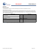
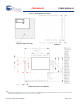
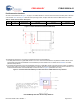
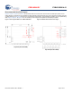
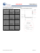
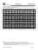
Table Of Contents
- EZ-BLE™ PRoC™ Bluetooth 4.2 Module
- General Description
- Benefits
- More Information
- Contents
- Overview
- Pad Connection Interface
- Recommended Host PCB Layout
- Power Supply Connections and Recommended External Components
- Electrical Specification
- Environmental Specifications
- Regulatory Information
- Packaging
- Ordering Information
- Acronyms
- Document Conventions
- Document History Page
- Sales, Solutions, and Legal Information

PRELIMINARY
CYBLE-222014-01
Document Number: 002-11186 Rev. ** Page 9 of 37
Table 4 details the solder pad connection definitions and available functions for each connection pad. Table 4 lists the solder pads on
CYBLE-222014-01, the BLE device port-pin, and denotes whether the function shown is available for each solder pad. Each
connection is configurable for a single option shown with a ✓.
Table 4. Solder Pad Connection Definitions
Solder Pad
Number
Device
Port Pin
UART SPI I
2
C TCPWM
[2]
CapSense
WCO
Out
ECO_OUT LCD SWD GPIO
1GND
[3]
Ground Connection
2P4.1
[4]
✓(CTS) ✓(MISO) ✓✓(Sensor /
C
TANK
)
✓✓
3P5.1✓(TX) ✓(SCLK) ✓(SCL) ✓✓(Sensor) ✓✓ ✓
4P5.0✓(RX) ✓(SS) ✓(SDA) ✓✓(Sensor) ✓✓
5V
DDR
Radio Power Supply (1.9V to 5.5V)
6P1.6
✓(RTS) ✓(SS) ✓✓(Sensor) ✓✓
7P0.7✓(CTS) ✓(SCLK) ✓✓(Sensor) ✓✓(SWDCLK) ✓
8P0.4✓(RX) ✓(MOSI) ✓(SDA) ✓✓(Sensor) ✓✓ ✓
9P0.5✓(TX) ✓(MISO) ✓(SCL) ✓✓(Sensor) ✓✓
10 GND Ground Connection
11 P0.6
✓(RTS) ✓(SS) ✓✓(Sensor) ✓✓(SWDIO) ✓
12 P1.7 ✓(CTS) ✓(SCLK) ✓✓(Sensor) ✓✓
13 V
DD
Digital Power Supply Input (1.71 to 5.5V)
14 XRES External Reset Hardware Connection Input
15 P3.5
✓(TX) ✓(SCL) ✓✓(Sensor) ✓✓
16 P3.4 ✓(RX) ✓(SDA) ✓✓(Sensor) ✓✓
17 P3.7 ✓(CTS) ✓(MISO) ✓(Sensor) ✓✓ ✓
18 P1.4 ✓(RX) ✓(MOSI) ✓(SDA) ✓✓(Sensor) ✓✓
19 P1.5 ✓(TX) ✓(MISO) ✓(SCL) ✓✓(Sensor) ✓✓
20 P3.6 ✓(RTS) ✓✓(Sensor) ✓✓
21 P4.0
[5]
✓(RTS) ✓(MOSI) ✓✓(C
MOD
) ✓✓
Notes
2. TCPWM stands for timer, counter, and PWM. If supported, the pad can be configured to any of these peripheral functions.
3. The main board needs to connect both GND connections (Pad 1 and Pad 10) on the module to the common ground of the system.
4. When using the capacitive sensing functionality, Pad 2 (P4.1) can be connected to a C
TANK
capacitor (located off of Cypress BLE Module). C
Tank
should be used
if implementing a shield layer on the capacitive sensor. If used, this capacitor should be placed as close to the module as possible.
5. When using the capacitive sensing functionality, Pad 21 (P4.0) must be connected to a C
MOD
capacitor (located off of Cypress BLE Module). The value of this
capacitor is 2.2 nF and should be placed as close to the module as possible.
6. If the I
2
S feature is used in the design, the I
2
S pins shall be dynamically routed to the appropriate available GPIO by PSoC Creator