
User's Manual
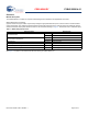
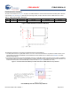
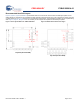
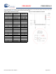
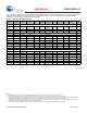
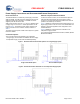
Table Of Contents
- EZ-BLE™ PRoC™ Bluetooth 4.2 Module
- General Description
- Benefits
- More Information
- Contents
- Overview
- Pad Connection Interface
- Recommended Host PCB Layout
- Power Supply Connections and Recommended External Components
- Electrical Specification
- Environmental Specifications
- Regulatory Information
- Packaging
- Ordering Information
- Acronyms
- Document Conventions
- Document History Page
- Sales, Solutions, and Legal Information

PRELIMINARY
CYBLE-222014-01
Document Number: 002-11186 Rev. ** Page 6 of 37
Pad Connection Interface
As shown in the bottom view of Figure 1 on page 5, the CYBLE-222014-01 connects to the host board via solder pads on the back
of the module. Tab le 2 and Figure 2 detail the solder pad length, width, and pitch dimensions of the CYBLE-222014-01 module.
Figure 2. Solder Pad Dimensions (Seen from Bottom)
To maximize RF performance, the host layout should follow these recommendations:
1. The ideal placement of the Cypress BLE module is in a corner of the host board with the chip antenna located at the far corner.
This placement minimizes the additional recommended keep out area stated in item 2. Please refer to AN96841 for module
placement best practices.
2. To maximize RF performance, the area immediately around the Cypress BLE module chip antenna should contain an additional
keep out area, where no grounding or signal traces are contained. The keep out area applies to all layers of the host board. The
recommended dimensions of the host PCB keep out area are shown in Figure 3 (dimensions are in mm).
Figure 3. Recommended Host PCB Keep Out Area Around the CYBLE-222014-01 Chip Antenna
Table 2. Solder Pad Connection Description
Name Connections Connection Type Pad Length Dimension Pad Width Dimension Pad Pitch
SP 22 Solder Pads 0.71 mm 0.41 mm 0.76 mm
Host PCB Keep Out Area Around Chip Antenna