
User's Manual

WD105
Datasheet
2014-03-20
11
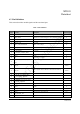
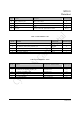
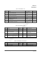
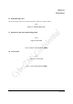
4.5 Pin Definitions
This section describes module signals and the associated pins.
Table 1: Pin Definitions
Pin No. Pin name Description Genernal Type
1 Ground Ground P
2 VDDIO_SDIO Connect to 3.3V host I/O supply or 1.8V peripheral I/O supply P
3 UART1_CTS|TDO UART Clear to Send O
4 TCK|I2C_CLK I2C Clock I/O
5 UART1_TXD|TESTMODE UART1 Series Output. O
6 UART1_RXD|TMS UART1 Series intput. I
7 I2C_DATA|TDI I2C DATA I/O
8 SPI_CLK|SD_CLK|I2S2_MCK
9 Ground Ground P
10 3.3V Connect to 3.3V supply P
11
SPI_MISO|SD_DATA0|I2S2_WS|JTA
G_EN
12 USB_DP
USB D+ signal; carries USB data to and from the USB 2.0
PHY
IA/OA
13 USB_DN
USB D- signal; carries USB data to and from the USB 2.0
PHY
IA/OA
14 SPI_INT|SD_DATA1|I2S2_SDO
15 SD_DATA2|I2S2_SDI|HM0
16 SPI_MOSI|SD_DATA3|I2S2_BCK
17 SPI_CS|SD_CMD|HM1
18 CHIP_PWD# Chip power-down control I
19 Ground Ground P
20 DVDD_GPIO Connect to 3.3V host I/O supply or 1.8V peripheral I/O supply P
21 GPIO23 General purpose input/output 23 I/O
22 I2S1_WS|TRST_8x8
23 UART1_RTS Bluetooth UART Request to Send. O