
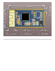
Product Description


TWI 1 Master
4.2.3 Flash Program I/Os
The module has two programmer pins, respectively SWDCLK pin and SWDIO pin. The two pin Serial Wire Debug (SWD) interface provided as a
part of the Debug Access Port (DAP) offers a flexible and powerful mechanism for non- intrusive debugging of program code. Breakpoints and
single stepping are part of this support.
4.2.4 Serial Peripheral Interface
The SPI interfaces enable full duplex synchronous communication between devices. They support a three-wire (SCK, MISO, MOSI) bi-directional
bus with fast data transfers. The SPI Master can communicate with multiple slaves using individual chip select signals for each of the slave devices
attached to a bus. Control of chip select signals is left to the application through use of GPIO signals. SPI Master has double buffered I/O data.
The SPI Slave includes EasyDMA for data transfer directly to and from RAM allowing Slave data transfers to occur while the CPU is IDLE. The
GPIOs are used for each SPI interface line can be chosen from any GPIOs on the device and independently. This enables great flexibility in device
pinout and efficient use of printed circuit board space and signal routing.
4.2.5 UARTs
The Universal Asynchronous Receiver/Transmitter offers fast, full-duplex, asynchronous serial communication with built-in flow control (CTS, RTS),
support in hardware up to 1 Mbps baud. Parity checking is supported. Support the following baudrate in bps unit:
1200/2400/4800/9600/14400/19200/28800/38400/57600/76800/115200.
Note: The GPIOs are used for each SPI/TWI/UART interface line can be chosen from any GPIOs on the device and configed independently.
4.2.6 Analog to Digital Converter (ADC)
The 12 bit incremental Analog to Digital Converter (ADC) enables sampling of up to 8 external signals through a front-end multiplexer. The ADC
has configurable input and reference prescaling, and sample resolution (8,10, and 12 bit).
Note: The ADC module uses the same analog inputs as the LPCOMP module. Only one of the modules can be enabled at the same time.
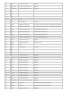
GourmetBlue BLE Module Pin Number Pin Number Description
4 P0.28 Digital I/O; Analog input 4
5 P0.29 Digital I/O; Analog input 5
6 P0.30 Digital I/O; Analog input 6
7 P0.31 Digital I/O; Analog input 7
24 P0.02 Digital I/O; Analog input 0
25 P0.03 Digital I/O; Analog input 1
26 P0.04 Digital I/O; Analog input 2
27 P0.05 Digital I/O; Analog input 3
4.2.7 Low Power Comparator (LPCOMP)
In System ON, the block can generate separate events on rising and falling edges of a signal, or sample the current state of the pin as being
above or below the threshold. The block can be configured to use any of the analog inputs on the device. Additionally, the low power comparator
can be used as an analog wakeup source from System OFF or System ON. The comparator threshold can be programmed to a range of fractions
of the supply voltage.
4.2.8 Reset
The reset pin of the GourmetBlue series module is in the internal pull-high state , when the reset pin of the module is input to a low level , the
module will be automatically reset .After the reset pin is used , the parameters of the current setting will not be reserved .
4.2.9 NFC