
User's Manual


CRXi
µ
µµ
µ
Core Module
CR
µ
µµ
µ
X Logic,
2001 all rights reserved
6
54 PD1 – U2 general purpose I/O
55 PD2 – U2 general purpose I/O
56 GND
Table 1
Pin Descriptions, Header J2
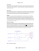
Header J2 is the 14 pin header on the CRXi board. It is used at the factory for initially programming and
testing of the CRXi. It gives direct JTAG access to the PLD section for chip decodes, memory mapping
scheme and other I/O configuration. The possibilities here are almost endless – Crux Logic could not begin
to support all the various memory maps, chip selects and logic that is possible with this device. We do not
support or recommend the user access or program the part through this port, although we wouldn’t
necessarily discourage it either. With proper knowledge and the required hardware, this is a valid means of
exploring the versatility of this part.
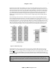
PIN DESCRIPTION
1NC
2NC
3 GND
4NC
5 PC5 – (JTAG TDI)
6 PC3 – (JTAG TSTAT)
7VCC
8/RESET
9 PC0 – (JTAG TMS)
10 GND
11 PC1 – (JTAG TCK)
12 GND
13 PC6 – (JTAG TDO)
14 PC4 – (JTAG /TERR)
Table 2
Pin Descriptions, Header J3
Header J3 is a 2 pin header located immediately above header J2. J3 is a jumper block used to control
access to the bootloader program. With no shorting jumper across these points, execution begins at ROM
address 0000h (user code) following a reset. With a shorting jumper installed across J3, the bootloader
program is invoked on a system reset, with this condition: assuming serial port communications are
properly connected, the bootloader will poll the serial port for a period of approximately 5 seconds after
reset. If no character is received within this time period, bootloader will exit and begin executing user code
at ROM address 0000h.
NOTE: Be advised that the bootloader is invoked after all resets regardless of the state of jumper J3. It is
the bootloader that is examining J3. This means the bootloader is using microcontroller resources
(internal RAM, registers and peripherals) even if jumper J3 is removed to allow user ROM code
execution. Therefor some registers and RAM will have data in them after a swap from bootloader to user
ROM. It is strongly urged that the user initialize internal RAM and registers to known values in the
beginning of their code.