
User's Manual

CRXi
µ
µµ
µ
Core Module
CR
µ
µµ
µ
X Logic,
2001 all rights reserved
4
Trademarks
Any brand and/or product names mentioned herein are trademarks or registered trademarks of their
respective holders.
Warranty
Every effort has been made to insure a quality, reliable product. If any defects in materials are evident
within a period of one year from the date of purchase Crux Logic will either , at its option, repair or replace
products or individual components which are deemed defective. If a product should fail after this period,
Crux Logic will repair or replace product at minimal cost. If product is deemed unacceptable for users
application, for whatever reason, within a period of one year, Crux Logic will refund in full the entire
amount of purchase, less shipping and handling, provided the item(s) are in working order. All shipping
and handling costs for are the responsibility of the customer.
Safe Handling
As with any microcontroller and high speed digital products, safe, static free handling is mandatory.
Controlling static and spurious noise/spikes is an obvious necessity in this environment , but sometimes its
easier said than done. Crux Logic’s products are built and tested in a static controlled environment and
shipped in static safe containers. Crux Logic recommends a static free workspace – static mats and
grounding straps are highly recommended. Static discharge is a large cause of damaged parts.
Features
As stated previously, the CRXi module is a state of the art microcontroller engine. It uses the latest 8051
architecture, flash ROM and non-volatile RAM (no battery required). Also on board is a serial bootloader.
The bootloader resides in a separate, protected memory space and has no effect on the final memory map.
!
Dallas Semiconductor 80C320 high speed micro
!
Executes 8051 instructions in 4 cycles as opposed to 12
!
Watchdog timer
!
Dual data pointer
!
32K of non-volatile RAM – will store data with no power, no battery needed
!
2048 bytes of additional scratchpad RAM (volatile – not available on all models)
!
Three 16 bit timer/counters
!
Two full duplex serial ports
!
128K flash ROM – second 64K accessed via on chip page register
!
Bootloader has no effect on memory map
!
Three decoded active low chip selects
!
Six general purpose memory mapped I/O
!
Combination fourteen general purpose I/O, serial ports or 6 external interrupt sources
!
Crystal and reset circuitry on board
Hardware
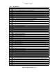
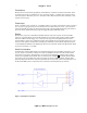
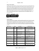
Pin Descriptions, Header J1
The header J1 is the 56 pin header running lengthwise along the board. Hole diameter is .040 inches. Pins
are on .100 inch centers, accepting a wide variety of connector types. A few of the pins are marked with
their pin numbers – these are pins 1 and 37, which are the VCC pins, and pins 20 and 56, which are the
GROUND pins. Many pins have multiple functions, for example pin 2 can be used for either uController
general purpose I/O port 1.0 or timer2 counter input. These are noted in the Table 1. U1 refers to the
microcontroller, U2 refers to the PSD/Flash and U3 refers to the RAM memory chip.