
User's Manual

CRXi
µ
µµ
µ
Core Module
CR
µ
µµ
µ
X Logic,
2001 all rights reserved
14
P
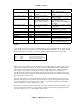
Sets memory page. By default, page is set to 0. This is indicated by the number preceding the prompt, as in
0>. After executing the command “P1” page one is selected and displayed as 1>. The selected page only
has effect on certain commands such as E (Erase), L(load), X(Examine code memory) and S(Run
checksum of selected memory page).
E
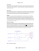
Erases selected memory page. If prompt shows 0>, entering “E” will erase page 0, address 0000h – FFFFh.
If page selected is 1 or 2 (prompt 1> or 2>), only the upper 32k bytes are erased in that selected page. The
only way to erase the common memory area addressed 0000h – 7FFFh is to have page 0 selected. See
Figure 2.
A
Erase all. Executing this command will erase the entire 128K Flash memory space.
L
Load Intel format .HEX file. After executing the “L” command, bootloader waits for the transfer of users
code (.hex) file. The prompt will change to “load .HEX file:”. See your terminal emulator program for
transferring a text file. There is no timeout period for receiving file. If user wishes to abort transfer after
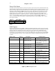
executing “L” command, CRXi must be reset. After load is executed, the load command returns certain
values. If successful load was performed, CRXi returns a value of 0, displayed as “LOAD ERR = 0”. See
Table 6 for details.
Value Description
0 Load successful
1 Flash write algorithm error
2 File checksum error
3 Write algorithm timeout error
4 End record checksum error
5 Flash memory not erased
Table 6
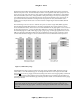
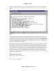
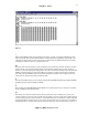
X
Examine, or dump selected flash ROM page code contents. This command takes two parameters – the
starting address and the ending address. See Figure 6.
S
Run checksum of selected flash ROM page.
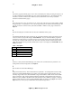
D
Dump external data memory. This command takes two parameters – the starting address and the ending
address. The selected flash ROM page has no effect on the output as this command displays only the
externally mapped data content. The NVSRAM is mapped from 0000h to 7FFFh. The area above 8000h
may be examined as well. Addresses 8000h to 8800h are additional scratchpad RAM. This scratchpad
RAM may not be available in all CRXi models. Not all addresses above 7FFFh are mapped, so dumping
memory in these areas may or may not yield predictable results. See memory map (Figure 2) for details.
Figure 6 shows a memory dump of NVSRAM contents 0000h through 00CCh.