
User's Manual

CRXi
µ
µµ
µ
Core Module
CR
µ
µµ
µ
X Logic,
2001 all rights reserved
11
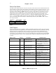
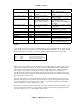
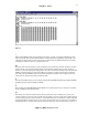
or output. output mode for NVSRAM access.
Must read all ones, FFh.
Direction – Port B C007h Configure Port B pin as input
or output.
0 = input, 1 = output. Default is 0
(input).
*Drive Select – Port A C008h Set pin as either CMOS or
open drain.
Do not change. Port A reserved as
address out mode.
Drive Select – Port B C009h Set pins 0 – 3 on Port B as
slow or fast slew rate, pins 4 –
7 as open drain or CMOS.
0 = slow slew rate, 1 = fast slew
rate. Default is 0 (slow). 0 =
CMOS, 1 = open drain. Default is
0 (CMOS).
Drive Select – Port C C016h Set pin as either CMOS or
open drain.
0 = CMOS, 1 = open drain. Default
is 0 (CMOS).
Drive Select – Port D C017h Set as fast or slow slew rate. 0 = slow slew rate, 1 = fast slew.
Default is 0 (slow slew rate).
Flash Protection C0C0h Flash Protection Read only
Flash Protection C0C2h Secondary Flash Protection Read only
PMMR0 C0B0h Power management register 0
PMMR2 C0B4h Power management register 2
Page C0E0h Page register Write to only bits0 and 1 (upper
bits of this register are reserved).
*VM C0E2h VM register Do not write to this register. It is
used to configure memory map.
Table 5
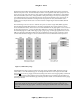
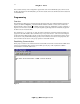
As an example, assume the user wants to use PB0 and PB1 as inputs, and PB2 and PB3 as outputs. We will
need to set bits 2 and 3 to 1, bits 0 and 1 to 0 and not affect the upper nibble, bits 4 – 7. This register resides
at data location C007h. The default is 0, so in this example we will assume the lower 4 bits are all 0.
Figure 3(Port B initialization example)
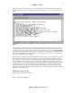
Now the user is free to write to bits PB2 and PB3, at location C005h (Data Out – Port B register) to set or
clear these bits as application requires. Also reads to input pins PB0 and PB1 at location C001h (Data In –
Port B register) can be performed. These external bytes are not bit addressable, so masking is necessary
when reading or writing to them. The above code would constitute a driver in its simplest form. In
assembly language, it could be suggested that the port drivers be put in macros to simplify the use of the
ports and to hide the details of the drivers. With a high level language, such as C, bitfields could make this
type of port bit access almost trivial.
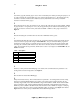
The drive select registers, locations C009h, C016h and C017h configures the pin driver as open drain or
CMOS for some port pins, and controls the slew rate for others. A pin can be configured for open drain if
its corresponding bit in the drive select register is set to a ‘1’. The default is CMOS. An external pullup
resistor should be used on pins configured as open drain.
Slew rate is the measurement of rise and fall times of an output. A higher slew rate means a faster response
and may create more electrical noise. A pin operates at a high slew rate when the corresponding bit in the
drive select register is set to a ‘1’. The default is slow slew rate.
movx dptr, #0C007h ;address of port B direction register
movx a, @dptr ;copy the contents of direction reg
xrl a, #0Ch ;exclusive or with mask and put in A
movx
@
d
p
tr
,
a
;
write it back to location C007h