
User's Manual


CRXi
µ
µµ
µ
Core Module
CR
µ
µµ
µ
X Logic,
2001 all rights reserved
10
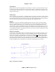
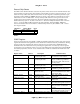
External Chip Selects
The CRXi comes standard with three active low chip selects. These can be used for external hardware such
as I/O expanders, keypad encoding, LCD interface, A/D and D/A converters to name a few. Pins 51 – 53 on
header J1 are chip selects /CS0, /CS1 and /CS2. These are each mapped to a 256 (FFh) byte address space
beginning at address 8800h (see Table 4). Reading or writing to these addresses will strobe the pin low to
select the device. This is a R/W strobe – the chip select pin will remain low as long as the read or write
signal from the microcontroller remains low. The lower eight bits of this address are available on the
latched address byte pins 39 – 46, PA0 – PA7. Pins 21 – 28 are the multiplexed data bus AD0 – AD7 and
pins 17 – 18 are the /WR and /RD signals from the microcontroller. Addresses 8B00h – BFFFh are
reserved and should not be read or written to. Additional chip selects may be available as well – contact
Crux Logic for details.
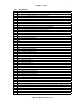
Chip Select Address Range Pin #
/CS0 8800h – 88FFh 51
/CS1 8900h – 89FFh 52
/CS2 8A00h – 8AFFh 53
Table 4
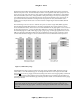
CSIOP Register
Occupying upper data space from C000h – C0FFh are the PSD configuration registers. Only a few of these
registers are needed for most applications. Some should not be written to under any circumstances. Writing
to these registers may undermine the integrity of the memory map, address bus to NVSRAM, and the
bootloader. These are noted below with a * preceding the register name. As noted, any writes to registers
involving Port A are not allowed, as Port A is set up as the latched low order address bus for the NVSRAM
and external peripherals (via /CS0 – /CS2). Addresses above C100h are undefined and should not be read
or written.
Register Name Address Description Additional Notes
*Data In – Port A C000h Reads port A pin as input,
MCU I/O input mode.
Not available to user – Port A used
for latched low order address.
Data In – Port B C001h Reads port B pin as input,
MCU I/O input mode.
4 locations – PB0 – PB3 (pins 47 –
50) are available as general I/O.
The upper 4, PB4 – PB7 are used
for chip selects.
Data In – Port C C010h Reads port C pin as input,
MCU I/O input mode.
Only PC2 (pin 38) is available as
general purpose I/O.
Data In – Port D C011h Reads port D pin as input,
MCU I/O input mode.
Only PD1 – PD2 (pins 54, 55)
available as general purpose I/O.
*Control – Port A C002h Select between I/O mode or
address out mode.
Do not change. Set as address out
mode for NVSRAM access. Must
read all ones, FFh.
Control – Port B C003h Select between I/O mode or
address out mode.
PB0 – PB3 available as general
purpose I/O.
*Data Out – Port A C004h Writes data to Port A (output). Do not use – Port A used for
address out.
Data Out – Port B C005h Writes data to Port B (output). Write to Port pin if corresponding
pin in Direction register is set to 1.
Data Out – Port C C012h Writes data to Port C (output). PC2 is output pin if corresponding
PC2 pin is set to 1 in Direction
register
Data Out – Port D C013h Writes data to Port D (output). Write to Port pin if corresponding
pin in Direction register is set to 1.
*Direction – Port A C006h Configure Port A pin as input Do not change. Set direction as