CRXi µCore Module CRµX Logic CRXi Manual For CRXi 122801.xxxxxxx, 22611.xxxxxxx Revision 5031.
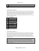
CRXi µCore Module INTRODUCTION............................................................................................................ 3 Overview .................................................................................................................................................3 About this manual ...................................................................................................................................3 Disclaimer .................................................
CRXi µCore Module 3 Introduction Overview Thank you for your purchase of the CRXi core module. The CRXi is a state of the art microcontroller “engine” used in small control and data acquisition products. On this small form factor, measuring 3 by 2 inches, are the processor, flash ROM, non-volatile RAM, crystal, reset circuitry and expansion connector.
CRXi µCore Module 4 Trademarks Any brand and/or product names mentioned herein are trademarks or registered trademarks of their respective holders. Warranty Every effort has been made to insure a quality, reliable product. If any defects in materials are evident within a period of one year from the date of purchase Crux Logic will either , at its option, repair or replace products or individual components which are deemed defective.
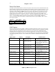
CRXi µCore Module PIN 1 2 3 4 5 6 7 8 9 10 11 12 13 14 15 16 17 18 19 20 21 22 23 24 25 26 27 28 29 30 31 32 33 34 35 36 37 38 39 40 41 42 43 44 45 46 47 48 49 50 51 52 53 DESCRIPTION VCC – 5 VDC power input P10 - U1 port 1.0 general purpose I/O or external I/O for timer/counter 2 P11 - U1 port 1.1 general purpose I/O or timer/counter 2 capture/reload trigger P12 - U1 port 1.2 general purpose I/O or serial port 1 input P13 - U1 port 1.3 general purpose I/O or serial port 1 output P14 - U1 port 1.
CRXi µCore Module 6 54 55 56 PD1 – U2 general purpose I/O PD2 – U2 general purpose I/O GND Table 1 Pin Descriptions, Header J2 Header J2 is the 14 pin header on the CRXi board. It is used at the factory for initially programming and testing of the CRXi. It gives direct JTAG access to the PLD section for chip decodes, memory mapping scheme and other I/O configuration.
CRXi µCore Module 7 Connections Because the end users hardware applications are all different, no headers are soldered to the board. These are inexpensive and easy to install. This is not a cost saving measure – we believe this provides for more connection options. All header pins are on .100 centers with a .040 hole diameter. This will satisfy a wide range of connector types. Power Input Power is supplied to pins on header J1. A regulated 5 VDC, ±.125 volts is recommended.
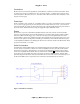
CRXi µCore Module 8 This diagram (Figure 1) completes the requirement for a ‘NULL’ connection and would require a straight non-null serial cable. If the connection was wired RXD to RXD and TXD to TXD, use of a NULL serial cable would be required. No special software is needed – communication is established through a standard terminal emulator. The default settings are 19200 bps, 8, N, 1. Consult Crux Logic for baud rates other than this default.
CRXi µCore Module 9 The flash area that contains the bootloader code consists of four 8K (2000h) segments and occupies the 80C320 code space at reset. It is automatically executed at reset regardless of the state of jumper J3. User has no access to this code space and it is write protected. The bootloader’s main function is downloading Intel .hex format files (users code), erasing the flash, reading and writing to memory and executing user code.
CRXi µCore Module 10 External Chip Selects The CRXi comes standard with three active low chip selects. These can be used for external hardware such as I/O expanders, keypad encoding, LCD interface, A/D and D/A converters to name a few. Pins 51 – 53 on header J1 are chip selects /CS0, /CS1 and /CS2. These are each mapped to a 256 (FFh) byte address space beginning at address 8800h (see Table 4). Reading or writing to these addresses will strobe the pin low to select the device.
CRXi µCore Module or output. Direction – Port B C007h Configure Port B pin as input or output. Set pin as either CMOS or open drain. Set pins 0 – 3 on Port B as slow or fast slew rate, pins 4 – 7 as open drain or CMOS. *Drive Select – Port A C008h Drive Select – Port B C009h Drive Select – Port C C016h Drive Select – Port D C017h Set pin as either CMOS or open drain. Set as fast or slow slew rate.
CRXi µCore Module 12 This is a brief summary of the configuration registers that reside in the CSIOP data space, and how to use the basic I/O functions of the PSD (Flash) part. For more detail, refer to the ST Microelectronics data sheet on the PSD913F2. Programming Overview Programming the CRXi part is performed through the boards serial port 0. Minimal isolation hardware is required, as outlined in Figure 1.
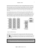
CRXi µCore Module 13 Note the prompt 0>. The 0 indicates we are on the default page 0. At this prompt the command set of the bootloader can be run. To see the available commands at any time, type ‘?’. A review of commands will follow. Figure 5 All commands are single characters. Some commands take parameters and these are shown in the text to the right of the character. For example, the W (Write) command takes 3 parameters. The first is the value you want to write.
CRXi µCore Module 14 P Sets memory page. By default, page is set to 0. This is indicated by the number preceding the prompt, as in 0>. After executing the command “P1” page one is selected and displayed as 1>. The selected page only has effect on certain commands such as E (Erase), L(load), X(Examine code memory) and S(Run checksum of selected memory page). E Erases selected memory page. If prompt shows 0>, entering “E” will erase page 0, address 0000h – FFFFh.
CRXi µCore Module 15 Figure 6 I Dump internal RAM contents. No parameters are necessary. A single ‘I’ command will dump the entire 80h (128 decimal) bytes of internal 8051 RAM. To maintain backward compatibility with the 8051, only 128 bytes are dumped. Note, however, that the 8032, which includes the Dallas 80C320 microcontroller, has 256 bytes of internal memory for general purpose use. W Write byte value to external memory. Three parameters are used with this command.
CRXi µCore Module the first address that contains an incorrect data value is returned. This test will also set all locations to 0 upon a successful exit, setting up the fourth test, a simple checksum, which should return 0. R Read 8051 register values. Read current contents of 8051 registers, along with the page register. Again, to maintain backward compatibility, the extended SFR registers of the 80C320 are not shown. G Execute user program at code address 0000h.