
Technical data


2-18 Diagnostic Procedures
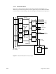
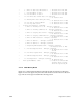
2.4.1.3 IO4 Interface Board
Figure 2-6 is a functional block diagram of the IO4 board and VCAM with the error
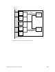
detection points called out. Figure 2-7 shows the physical layout of the IO4 board and the
locations of the error detection logic. The error messages are listed in the following section.
Figure 2-6 IO4/VCAM Board Error Detection Logic
(256 + 8 Parity)
Ebus Data
Ebus Addr/Cmd
ID
ASIC
ID
ASIC
Ibus
EPC
F chip
SCSI 0
Ethernet
Parallel Port
Core I/O
Graphics
VCAM Board
VMEbus
IO4 Board
12
910
7
F chip
8
9
VMECC
8
9
S1
5
6
Addr/Data
(64 + 4 Parity)
(48 + 2 Parity)
SCSI 1
SCSI 2
Data (16 + 2 Parity)
10
11
FCI Data
(32 + 2 Parity)
Board Set
FCI Data
(32 + 2 Parity)
chip
ID
ASIC
34
ID
ASIC
78
16+1 Parity
16+1 Parity
13
Map RAM
(SRAM)
12
12
IA
ASIC
56