
Technical data

2-8 Diagnostic Procedures
2.4.1.1 IP19 CPU Board
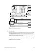
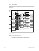
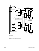
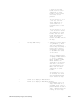
Figure 2-2 is a functional block diagram of the IP19 board with the error detection points
called out. Figure 2-3 shows the physical layout of the board and the locations of the error
detection logic.
Figure 2-2 IP19 Board Error Detection Logic
Note: Because each of the four processor slices are identical, only the registers
corresponding to slice 0 are described in the following section.
Eb
us
Data
Ebus
Addr
Data (64 + 4 Parity) Data (24 + 4 Parity)
Addr/Data (64 + 8 ECC)
Addr (17 + 1 Parity)
Addr/Cmd (48 + 2 Parity)
Data (256 + 8 Parity)
D
ASIC
D
ASIC
A
ASIC
D
ASIC
D
ASIC
67
12
35
4
CC
CHIP
CC
CHIP
CC
CHIP
CC
CHIP
SRAM
(Bus Tags)
SRAM
(Bus Tags)
SRAM
(Bus Tags)
SRAM
(Bus Tags)
CPU 0
and
SCache
CPU 0
and
SCache
CPU 0
and
SCache
CPU 0
and
SCache