
Data Sheet

1/7September 2001
■ PROPAGATION DELAY TIME
t
PD
= 60ns (Typ.) at V
DD
= 10V
■ BUFFERED INPUTS AND OUTPUTS
■ STANDARDIZED SYMMETRICAL OUTPUT
CHARACTERISTICS
■ QUIESCENT CURRENT SPECIFIED UP TO
20V
■ 5V, 10V AND 15V PARAMETRIC RATINGS
■ INPUT LEAKAGE CURRENT
I
I
= 100nA (MAX) AT V
DD
= 18V T
A
= 25°C
■ 100% TESTED FOR QUIESCENT CURRENT
■ MEETS ALL REQUIREMENTS OF JEDEC
JESD13B " STANDARD SPECIFICATIONS
FOR DESCRIPTION OF B SERIES CMOS
DEVICES"
DESCRIPTION
The HCF4011B is a monolithic integrated circuit
fabricated in Metal Oxide Semiconductor
technology available in DIP and SOP packages.
The HCF4011B QUAD 2 INPUT NAND GATE
provides the system designer with direct
implementation of the NAND function and
supplement the existing family of CMOS gates. All
inputs and outputs are buffered.
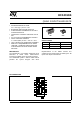
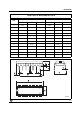
HCF4011B
QUAD 2 INPUT NAND GATE
PIN CONNECTION
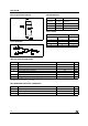
ORDER CODES
PACKAGE TUBE T & R
DIP HCF4011BEY
SOP HCF4011BM1 HCF4011M013TR
DIP SOP