
Data Sheet
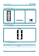
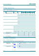
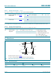
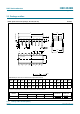
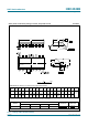
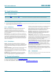
Table Of Contents
- 1. General description
- 2. Features
- 3. Applications
- 4. Ordering information
- 5. Functional diagram
- 6. Pinning information
- 7. Functional description
- 8. Limiting values
- 9. Recommended operating conditions
- 10. Static characteristics
- 11. Dynamic characteristics
- 12. Waveforms
- 13. Package outline
- 14. Abbreviations
- 15. Revision history
- 16. Legal information
- 17. Contact information
- 18. Contents

HEF4049B_5 © NXP B.V. 2008. All rights reserved.
Product data sheet Rev. 05 — 11 November 2008 8 of 11
NXP Semiconductors
HEF4049B
Hex inverting buffers
Fig 8. Package outline SOT109-1 (SO16)
X
w M
θ
A
A
1
A
2
b
p
D
H
E
L
p
Q
detail X
E
Z
e
c
L
v M
A
(A )
3
A
8
9
1
16
y
pin 1 index
UNIT
A
max.
A
1
A
2
A
3
b
p
cD
(1)
E
(1) (1)
eH
E
LL
p
QZywv θ
REFERENCES
OUTLINE
VERSION
EUROPEAN
PROJECTION
ISSUE DATE
IEC JEDEC JEITA
mm
inches
1.75
0.25
0.10
1.45
1.25
0.25
0.49
0.36
0.25
0.19
10.0
9.8
4.0
3.8
1.27
6.2
5.8
0.7
0.6
0.7
0.3
8
0
o
o
0.25 0.1
DIMENSIONS (inch dimensions are derived from the original mm dimensions)
Note
1. Plastic or metal protrusions of 0.15 mm (0.006 inch) maximum per side are not included.
1.0
0.4
SOT109-1
99-12-27
03-02-19
076E07 MS-012
0.069
0.010
0.004
0.057
0.049
0.01
0.019
0.014
0.0100
0.0075
0.39
0.38
0.16
0.15
0.05
1.05
0.041
0.244
0.228
0.028
0.020
0.028
0.012
0.01
0.25
0.01 0.004
0.039
0.016
0 2.5 5 mm
scale
SO16: plastic small outline package; 16 leads; body width 3.9 mm
SOT109-1