
Data Sheet
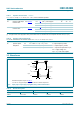
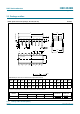
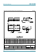
Table Of Contents
- 1. General description
- 2. Features
- 3. Applications
- 4. Ordering information
- 5. Functional diagram
- 6. Pinning information
- 7. Functional description
- 8. Limiting values
- 9. Recommended operating conditions
- 10. Static characteristics
- 11. Dynamic characteristics
- 12. Waveforms
- 13. Package outline
- 14. Abbreviations
- 15. Revision history
- 16. Legal information
- 17. Contact information
- 18. Contents

HEF4049B_5 © NXP B.V. 2008. All rights reserved.
Product data sheet Rev. 05 — 11 November 2008 4 of 11
NXP Semiconductors
HEF4049B
Hex inverting buffers
10. Static characteristics
11. Dynamic characteristics
Table 6. Static characteristics
V
SS
= 0 V; V
I
= V
SS
or V
DD
unless otherwise specified.
Symbol Parameter Conditions V
DD
T
amb
= −40 °C T
amb
= 25 °C T
amb
= 85 °C Unit
Min Max Min Max Min Max
V
IH
HIGH-level input voltage |I
O
| < 1 µA 5 V 3.5 - 3.5 - 3.5 - V
10 V 7.0 - 7.0 - 7.0 - V
15 V 11.0 - 11.0 - 11.0 - V
V
IL
LOW-level input voltage |I
O
| < 1 µA 5 V - 1.5 - 1.5 - 1.5 V
10 V - 3.0 - 3.0 - 3.0 V
15 V - 4.0 - 4.0 - 4.0 V
V
OH
HIGH-level output voltage |I
O
| < 1 µA 5 V 4.95 - 4.95 - 4.95 - V
10 V 9.95 - 9.95 - 9.95 - V
15 V 14.95 - 14.95 - 14.95 - V
V
OL
LOW-level output voltage |I
O
| < 1 µA 5 V - 0.05 - 0.05 - 0.05 V
10 V - 0.05 - 0.05 - 0.05 V
15 V - 0.05 - 0.05 - 0.05 V
I
OH
HIGH-level output current V
O
= 2.5 V 5 V −1.7 - −1.4 - −1.1 - mA
V
O
= 4.6 V 5 V −0.52 - −0.44 - −0.36 - mA
V
O
= 9.5 V 10 V −1.3 - −1.1 - −0.9 - mA
V
O
= 13.5 V 15 V −3.6 - −3.0 - −2.4 - mA
I
OL
LOW-level output current V
O
= 0.4 V 4.75 V 3.5 - 2.9 - 2.3 - mA
V
O
= 0.5 V 10 V 12.0 - 10.0 - 8.0 - mA
V
O
= 1.5 V 15 V 24.0 - 20.0 - 16.0 - mA
I
I
input leakage current V
DD
= 15 V 15 V - ±0.3 - ±0.3 - ±1.0 µA
I
DD
supply current I
O
= 0 A 5 V - 4.0 - 4.0 - 30 µA
10 V - 8.0 - 8.0 - 60 µA
15 V - 16.0 - 16.0 - 120 µA
C
I
input capacitance - - - 7.5 - - pF
Table 7. Dynamic characteristics
V
SS
= 0 V; C
L
= 50 pF; t
r
= t
f
≤
20 ns; T
amb
= 25
°
C; unless otherwise specified.
Symbol Parameter Conditions V
DD
Extrapolation formula Min Typ Max Unit
t
PHL
HIGH to LOW
propagation delay
nA to nY;
see
Figure 5
5 V
[1]
26 ns + (0.18 ns/pF)C
L
-3570ns
10 V 11 ns + (0.08 ns/pF)C
L
-1530ns
15 V 9 ns + (0.05 ns/pF)C
L
-1225ns
t
PLH
LOW to HIGH
propagation delay
nA to nY;
see
Figure 5
5 V
[1]
23 ns + (0.55 ns/pF)C
L
- 50 100 ns
10 V 14 ns + (0.23 ns/pF)C
L
-2550ns
15 V 12 ns + (0.16 ns/pF)C
L
-2040ns