
Data Sheet
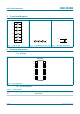
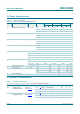
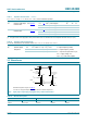
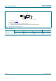
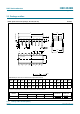
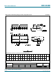
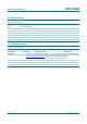
Table Of Contents
- 1. General description
- 2. Features
- 3. Applications
- 4. Ordering information
- 5. Functional diagram
- 6. Pinning information
- 7. Functional description
- 8. Limiting values
- 9. Recommended operating conditions
- 10. Static characteristics
- 11. Dynamic characteristics
- 12. Waveforms
- 13. Package outline
- 14. Abbreviations
- 15. Revision history
- 16. Legal information
- 17. Contact information
- 18. Contents

HEF4049B_5 © NXP B.V. 2008. All rights reserved.
Product data sheet Rev. 05 — 11 November 2008 2 of 11
NXP Semiconductors
HEF4049B
Hex inverting buffers
5. Functional diagram
6. Pinning information
6.1 Pinning
6.2 Pin description
Fig 1. Logic symbol Fig 2. Logic diagram for one gate Fig 3. Input protection circuit
001aai331
3
1A 1Y
2
5
2A 2Y
4
7
3A 3Y
6
9
4A 4Y
10
11
5A 5Y
12
14
6A 6Y
15
mna341
A
Y
001aae604
input
V
SS
Fig 4. Pin configuration
HEF4049B
V
DD
n.c.
1Y 6Y
1A 6A
2Y n.c.
2A 5Y
3Y 5A
3A 4Y
V
SS
4A
001aae602
1
2
3
4
5
6
7
8
10
9
12
11
14
13
16
15
Table 2. Pin description
Symbol Pin Description
V
DD
1 supply voltage
1Y to 6Y 2, 4, 6, 10, 12, 15 output