
Data Sheet
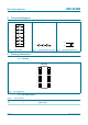
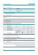
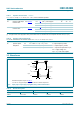
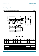
Table Of Contents
- 1. General description
- 2. Features
- 3. Applications
- 4. Ordering information
- 5. Functional diagram
- 6. Pinning information
- 7. Functional description
- 8. Limiting values
- 9. Recommended operating conditions
- 10. Static characteristics
- 11. Dynamic characteristics
- 12. Waveforms
- 13. Package outline
- 14. Abbreviations
- 15. Revision history
- 16. Legal information
- 17. Contact information
- 18. Contents

1. General description
The HEF4049B provides six inverting buffers with high current output capability suitable
for driving TTL or high capacitive loads. Since input voltages in excess of the buffers’
supply voltage are permitted, the buffers may also be used to convert logic levels of up to
15 V to standard TTL levels. Their guaranteed fan-out into common bipolar logic elements
is shown in Table 3.
It operates over a recommended V
DD
power supply range of 3 V to 15 V referenced to V
SS
(usually ground). Unused inputs must be connected to V
DD
, V
SS
, or another input. It is
also suitable for use over the industrial (−40 °C to +85 °C) temperature range.
2. Features
n Accepts input voltages in excess of the supply voltage
n Fully static operation
n 5 V, 10 V, and 15 V parametric ratings
n Standardized symmetrical output characteristics
n Operates across the full industrial temperature range −40 °C to +85 °C
n Complies with JEDEC standard JESD 13-B
n ESD protection:
u HBM JESD22-A114E exceeds 2000 V
u MM JESD22-A115-A exceeds 200 V
3. Applications
n LOCMOS (Local Oxidation CMOS) to DTL/TTL converter
n HIGH sink current for driving two TTL loads
n HIGH-to-LOW level logic conversion
4. Ordering information
HEF4049B
Hex inverting buffers
Rev. 05 — 11 November 2008 Product data sheet
Table 1. Ordering information
All types operate from
−
40
°
C to +85
°
C.
Type number Package
Name Description Version
HEF4049BP DIP16 plastic dual in-line package; 16 leads (300 mil) SOT38-4
HEF4049BT SO16 plastic small outline package; 16 leads; body width 3.9 mm SOT109-1