
Datasheet


TIC225A, TIC225B, TIC225C, TIC225D, TIC225E, TIC225M,
TIC225N, TIC225S
Page 2 of 3
SEMICONDUCTORS
Notes:
1. These values apply bidirectionally for any value of resistance between the gate and Main Terminal
1.
2. This value applies for 50-Hz full-sine-wave operation with resistive load. Above 70°C derate
linearly to 110°C case temperature at the rate of 200 mA/°C.
3. This value applies for one 50-Hz full-sine-wave when the device is operating at (or below) the rated
value of on-state current. Surge may be repeated after the device has returned to original thermal
equilibrium. During the surge, gate control may be lost.
4. This value applies for one 50-Hz half-sine-wave when the device is operating at (or below) the rated
value of on-state current. Surge may be repeated after the device has returned to original thermal
equilibrium. During the surge, gate control may be lost.
5. This value applies for a maximum averaging time of 20 ms.
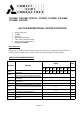
THERMAL CHARACTERISTICS
Symbol Ratings Value Unit
R
∂JC
Junction to case thermal resistance ≤ 2.5
R
∂JA
Junction to free air thermal resistance ≤ 62.5
°C/W
ELECTRICAL CHARACTERISTICS
TC=25°C unless otherwise noted
Symbol Ratings
Test Condition(s)
Min Typ Mx Unit
I
DRM
Repetitive peak off-
state current
V
D
= Rated V
DRM
, , I
G
= 0,
T
C
= 110°C
- - ±2 mA
V
supply
= +12 V†, R
L
= 10 Ω, t
p(g)
= > 20 µs
- 0.8 5
V
supply
= +12 V†, R
L
= 10 Ω, t
p(g)
= > 20 µs
- -4.5 -20
V
supply
= -12 V†, R
L
= 10 Ω, t
p(g)
= > 20 µs
- -3.5 -10
I
GT
Gate trigger current
V
supply
= -12 V†, R
L
= 10 Ω, t
p(g)
= > 20 µs
- 11.7 30
mA
V
supply
= +12 V†, R
L
= 10 Ω, t
p(g)
= > 20 µs
- 0.7 2
V
supply
= +12 V†, R
L
= 10 Ω, t
p(g)
= > 20 µs
- -0.8 -2
V
supply
= -12 V†, R
L
= 10 Ω, t
p(g)
= > 20 µs
- -0.8 -2
V
GT
Gate trigger voltage
V
supply
= -12 V†, R
L
= 10 Ω, t
p(g)
= > 20 µs
- 0.9 2
V
V
supply
= +12 V†, I
G
= 0,
initiating I
TM
= 100 mA
- 3 20
I
H
Holding current
V
supply
= -12 V†, I
G
= 0,
initiating I
TM
= -100 mA
- -4.7 -20
mA
V
supply
= +12 V† (seeNote7) - - 30
I
L
Latching current
V
supply
= -12 V† (seeNote7) - - -30
mA
V
TM
Peak on-state voltage I
TM
= ± 12 A, I
G
= 50 mA (see Note6) - ±1.6 ±2.1 V
dv/dt
Critical rate of rise of
off-state voltage
V
DRM
= Rated V
DRM
, I
G
= 0
T
C
= 110°C
- ±50 -
dv/dt
©
Critical rise of
communication voltage
V
DRM
= Rated V
DRM
, I
TRM
= ± 12A
T
C
= 70°C
±1 ±1.5 ±4.5
V/µs
† All voltages are whit respect to Main Terminal 1.