
Specifications


4–10 Functional Description
9 March 1999 – Subject To Change
Interrupts
4.3.5 Flash ROM Address Map
The address range for the flash ROM is FFF8.0000–FFFF.FFFF. Flash space of 1MB
is obtained by double mapping this 512KB space. FLASH_ADR19 register at I/O
location 800
16
provides this function. Writing a 0 to this location enables the lower
512KB of flash. Writing a 1 to this location enables the upper 512KB of flash.
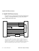
4.4 Interrupts
This section describes the AlphaPC 164LX interrupt logic. PCI-, ISA-, and 21174-
generated interrupts are described. Figure 4–5 shows the interrupt logic.
The PCI-to-ISA SIO bridge chip provides the functionality of two 8259 interrupt
control devices. These ISA-compatible interrupt controllers are cascaded so that 14
external and 2 internal interrupts are available. The PCI interrupt acknowledge com-
mand should be used to read the interrupt request vector from the SIO.
However, the AlphaPC 164LX system has more external interrupts than the SIO can
handle. Therefore, all the ISA interrupts are sent to the SIO except for the two 21174
interrupts, the TOY interrupt, the IDE controller interrupt, and the 16 PCI interrupts.
They are sent to an external interrupt programmable logic array (PLA). This PLA
takes these interrupts, as well as an OR of the nonexistent memory (NMI) and error
signals from the SIO, and generates pci_isa_irq. During reset, cpu_irq<3:0> con-
vey the system clocking ratios and delays, which are set by jumpers on J27.
Table 4–2 lists each system interrupt, its fixed interrupt priority level (IPL), and its
AlphaPC 164LX implementation. Table 4–3 lists each ISA bus interrupt and its
AlphaPC 164LX implementation.
800 FLASH_ADR19 register
801 AlphaPC 164LX configuration register
804-806 PCI interrupt registers
Table 4–1 ISA I/O Address Map (Continued)
Range (hex) Usage