
Specifications


9 March 1999 – Subject To Change
Functional Description 4–5
21174 Core Logic Chip
The AlphaPC 164LX supports a maximum of 512MB of main memory. The memory
is organized as two banks. Table 1–1 lists total memory options along with the corre-
sponding DIMM sizes required. All CPU cacheable memory accesses and PCI DMA
accesses are controlled and routed to main memory by the 21174 core logic chip.
The AlphaPC 164LX implements the alternate memory mode for SDRAM RAS
and CAS control signals. Alternate memory mode is explained in the 21174 Core
Logic Chip Technical Reference Manual.
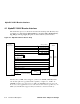
4.2.3 PCI Devices
The AlphaPC 164LX uses the PCI bus as the main I/O bus for the majority of periph-
eral functions. As Figure 4–3 shows, the board implements the ISA bus as an expan-
sion bus for system support functions and for relatively slow peripheral devices.
Figure 4–3 AlphaPC 164LX PCI Bus Devices
The PCI bus supports multiplexed, burst mode, read and write transfers. It sup-
ports synchronous operation of 33 MHz. It also supports either a 32-bit or 64-bit
data path with 32-bit device support in the 64-bit configuration. Depending upon
FM-05947.AI4
21174
pc164lx.7
82378ZB
pc164lx.22
pc164lx.18
PCI0646
SIO Bridge
IDE Controller
PCI Bus
PCI
Slot 0
J26
PCI
PCI
Slot 1
Slot 2
J23
J17
PCI
Slot 3
J16
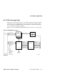
Device IDSEL Select
pci_ad16
pci_ad17
pci_ad18
pci_ad19
pci_ad20
pci_ad21
pci_ad22
Slot 2
Slot 0
Slot 1
SIO Bridge
Slot 3
Reserved
IDE Control
J7 J6
ISA Bus
Primary
Secondary