
Specifications


4–4 Functional Description
9 March 1999 – Subject To Change
21174 Core Logic Chip
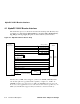
4.2.1 21174 Chip Overview
The 21174 application-specific integrated circuit (ASIC) accepts addresses and com-
mands from the 21164 microprocessor and drives the main memory array with the
address, control, and clock signals. It also provides an interface to the 64-bit PCI I/O
bus.
The 21174 chip provides the following functions:
• Serves as the interface between the 21164 microprocessor, main memory
(addressing and control), and the PCI bus. A three-entry CPU instruction queue
is implemented to capture commands should the memory or I/O port be busy.
• Provides control to the Quick Switch chips to isolate the L3 cache from the main
memory bus during private reads and writes.
• Generates the clocks, row, and column addresses for the SDRAM DIMMs, as
well as all of the memory control signals (RAS, CAS, WE). All of the required
SDRAM refresh control is contained in the 21174.
• Provides all the logic to map 21164 noncacheable addresses to PCI address
space, as well as all the translation logic to map PCI DMA addresses to system
memory.
Two DMA conversion methods are supported:
• Direct mapping, in which a base offset is concatenated with the PCI address.
• Scatter-gather mapping, which maps an 8KB PCI page to any 8KB memory
page. The 21174 contains an eight-entry scatter-gather translation lookaside
buffer (TLB), where each entry holds four consecutive page table entries (PTEs).
Refer to Appendix A for additional details on PCI and DMA address mapping.
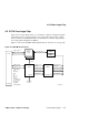
4.2.2 Main Memory Interface
Sixteen Quick Switches provide the interface between the 21164/L3 cache
(data_h<127:0>, check_h<15:0>) and the memory/21174 (mem_data_h<127:0>,
mem_check_h<15:0>). The AlphaPC 164LX supports four 168-pin unbuffered 72-bit
SDRAM DIMM modules. Quadword ECC is supported on the SDRAM and CPU
buses. Even parity is generated on the PCI bus.