
Specifications

2–6 System Configuration and Connectors
9 March 1999 – Subject To Change
Flash ROM Update Jumper (J28)
2.6 Flash ROM Update Jumper (J28)
When J28–2/3 are jumpered together (default), the flash ROM is write-enabled.
When J28–1/2 are jumpered together, the flash ROM is write-protected.
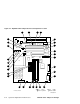
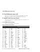
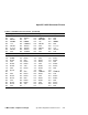
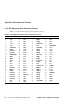
2.7 AlphaPC 164LX Connector Pinouts
This section lists the pinouts of all AlphaPC 164LX connectors. See Figure 2–1 for
connector locations.
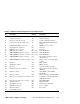
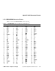
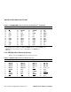
2.7.1 PCI Bus Connector Pinouts
Table 2–2 shows the PCI bus connector pinouts.
Table 2–2 PCI Bus Connector Pinouts
Pin Signal Pin Signal Pin Signal Pin Signal
32-Bit and 64-Bit PCI Connectors (J16, J17, J23, J26)
A1 TRST# A2 +12V A3 TMS A4 TDI
A5 Vdd A6 INTA A7 INTC A8 Vdd
A9 —A10Vdd A11 — A12 Gnd
A13 Gnd A14 — A15 RST# A16 Vdd
A17 GNT# A18 Gnd A19 — A20 AD<30>
A21 +3V A22 AD<28> A23 AD<26> A24 Gnd
A25 AD<24> A26 IDSEL A27 +3V A28 AD<22>
A29 AD<20> A30 Gnd A31 AD<18> A32 AD<16>
A33 +3V A34 FRAME# A35 Gnd A36 TRDY#
A37 STOP# A38 STOP# A39 +3V A40 SDONE
A41 SBO# A42 Gnd A43 PAR A44 AD<15>
A45 +3V A46 AD<13> A47 AD<11> A48 Gnd
A49 AD<09> A50 Not used A51 Not used A52 C/BE#<0>
A53 +3V A54 AD<06> A55 AD<04> A56 Gnd
A57 AD<02> A58 AD<00> A59 Vdd A60 REQ64#
A61 Vdd A62 Vdd B1 –12V B2 TCK
B3 Gnd B4 TDO B5 Vdd B6 Vdd
B7 INTB B8 INTD B9 PRSNT1# B10 —
B11 PRSNT2# B12 Gnd B13 Gnd B14 —
B15 Gnd B16 CLK B17 Gnd B18 REQ#
B19 Vdd B20 AD<31> B21 AD<29> B22 Gnd
B23 AD<27> B24 AD<25> B25 +3V B26 C/BE#<3>