
Specifications


9 March 1999 – Subject To Change
System Address Space A–45
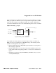
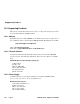
Suggested Use of a PCI Window
Table A–15 lists the PCI window power-up configuration characteristics.
A.16.1 Peripheral Component Architecture Compatibility Addressing and Holes
The peripheral component architecture allows certain (E)ISA devices to respond to
hardwired memory addresses. An example is a VGA graphics device that has its
frame buffer located in memory address region A0000–BFFFF. Such devices
“pepper” memory space with holes, which are collectively known as peripheral com-
ponent compatibility holes.
The PCI-EISA bridge decodes PCI addresses and generates a signal, mem_cs_l,
which takes into account the various PC compatibility holes.
A.16.2 Memory Chip Select Signal mem_cs_l
The PCI-EISA bridge can be made using the following two chips:
• Intel 82374EB EISA System Component (ESC)
• Intel 82375EB PCI-EISA Bridge (PCEB)
The PCI-EISA bridge provides address decode logic with considerable attributes
(such as read only, write only, VGA frame buffer, memory holes, and BIOS shadow-
ing) to help manage the EISA memory map and peripheral component compatibility
holes.
This is known as main memory decoding in the PCI-EISA chip, and results in the
generation of the memory chip select (mem_cs_l) signal. One exception is the VGA
memory hole region that never asserts mem_cs_l. If enabled, the 21174 uses this sig-
nal with the W0_BASE register.
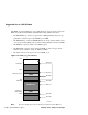
In Figure A–23, the two main holes are shown lightly shaded, while the mem_cs_l
range is darkly shaded.
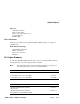
Table A–15 PCI Window Power-Up Configuration
PCI Window Assignment Size Comments
0 Scatter-gather 8MB Not used by firmware; mem_cs_l disabled
1 Direct-mapped 1GB Mapped to 0GB to 1GB of main memory
2 Disabled ——
3 Disabled — —