
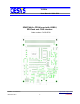
Electronic Keyboard User Manual
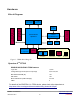

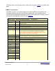

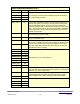

LPDDR SDRAM MT46H64M16LFCK-5
Signal Name FPGA IO Comment
MCB1_RAS_n K15
Command inputs: RAS#, CAS#, and WE# (along with CS#) define
the command being entered. *
MCB1_CAS_n K16
MCB1_WE_n K12
MCB1_CS_n --
MCB1_CKE_n D17 Clock enable: CKE HIGH activates, and CKE LOW deactivates, the
internal clock signals, input buffers, and output drivers. Taking CKE
LOW enables PRECHARGE power-down and SELF REFRESH
operations (all banks idle), or ACTIVE power-down (row active in any
bank). CKE is synchronous for all functions except SELF REFRESH
exit. All input buffers (except CKE) are disabled during power-down
and self refresh modes.
MCB1_RZQ N14 Input termination calibration pin used with the soft calibration module.
External 100 Ohm resistor to GND.
MCB1_ZIO No connect signal used with the soft calibration module to calibrate
the input termination value.
MCB1_CK G16 Clock: CK is the system clock input. CK and CK# are differential
clock inputs. All address and control input signals are sampled on the
crossing of the positive edge of CK and the negative edge of CK#.
Input and output data is referenced to the crossing of CK and CK#
(both directions of the crossing).
MCB1_CK_n G18
MCB1_DQ0 M16
Data input/output: Lower Byte Data bus.
MCB1_DQ1 M18
MCB1_DQ2 L17
MCB1_DQ3 L18
MCB1_DQ4 H17
MCB1_DQ5 H18
MCB1_DQ6 J16
MCB1_DQ7 J18
MCB1_LDQS K17 Data strobe for Lower Byte Data bus: Output with read data, input
with write data. DQS is edge-aligned with read data, center-aligned in
write data. It is used to capture data.
MCB1_LDM L16 Input data mask: DM is an input mask signal for write data. Input data
is masked when DM is sampled HIGH along with that input data
during a WRITE access. DM is sampled on both edges of DQS.
MCB1_UDM L15
MCB1_DQ8 N17 Data input/output: Upper Byte Data bus.
MCB1_DQ9 N18
MCB1_DQ10 P17
MCB1_DQ11 P18
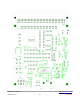
USBS6 / C1030-5510 http://www.cesys.com/
User Doc V0.3 -10- preliminary