CMX-ZG03 Datasheet (VER.0.
RISE Data Sheet : CMX-ZG03 ZigBee 3.0 , ZigBee PRO and IEEE802.15.4 Module Overview CMX-ZG03 using the IEEE802.15.4 standard in the 2.4 GHz - 2.5 GHz ISM frequency band, including ZigBee 3.0 and ZigBee PRO stack with Home Automation, Light Link and Smart Energy profiles. The modules integrate all of the RF components required, removing the need to perform expensive RF design and test. Products can be designed by simply connecting sensors and switches to the module IO pins.
RISE Benefits • • • • Microminiature module solutions Ready to use in products Minimises product development time No RF test required for systems Applications • • • • • Robust and secure low-power wireless applications ZigBee Smart Energy networks ZigBee Home Automation networks Toys and gaming peripherals Energy harvesting - for example, self-powered light switch Features: Module • 2.4GHz IEEE 802.15.4, , ZigBee 3.
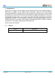
RISE Contents 1. Introduction ……………………………………………………………………………………5 1.1. Variants…………………………………………………………………………………………………….. 5 2. Specifications………………………………………………………………………………….6 3. Product Development………………………………………………………………………...7 3.1. JN5XXX Single Chip Wireless Microcontroller……………..……………………….…………….…….7 4. Pin Configurations………………………………………………………….………….…..…8 4.1. Pin Assignment……………………………………………………………………………………..….…. 9 4.2. Pin Descriptions………………………………..……………………………………………………...… 12 4.2.
RISE 1. Introduction CMX-ZG03 is a range of ultra-low power, high performance surface mount modules targeted at IEEE 802.15.4, ZigBee 3.0 and ZigBee Home Automation, Light Link and Smart Energy networking applications, enabling users to realize products with minimum time to market and at the lowest cost. They remove the need for expensive and lengthy development of custom RF board designs and test suites.
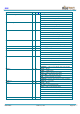
RISE 2. Specifications VDD=3.0V @ +25°C Typical DC Characteristics Notes CMX-ZG03 Deep sleep current 70nA Sleep current Radio transmit current Radio receive current 0.73uA In sleep mode; with I/O and RC oscillator timer wake-up; 25mA 10dBm @2.8V Maximu input level at 10dBm 17.8mA Centre frequency accuracy Additional +/-15ppm allowance for temperature and ageing +/-25ppm Typical RF Characteristics Receive sensitivity Nominal for 1% PER, as per 802.15.4 section 6.5.3.
RISE Programmable analogue comparators 1 Internal temperature sensor and battery monitor 1 Ultra low power mode for sleep 3. Product Development A range of evaluation/developer kits is also available, allowing products to be quickly bread boarded. Efficient development of software applications is enabled by the provision of a complete, unlimited, software developer kit. Together with the available libraries for the IEEE802.15.
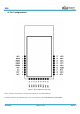
RISE 4. Pin Configurations Figure 1: Pin Configuration (top view) Note : that the same basic pin configuration applies for all module designs. However, DIO2 (pin 8) and DIO3 (pin 9) are not available on the RZN-AEM00 and RZN-AEM05. CMX-ZG03 RISE CO., LTD.
RISE 4.1.
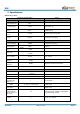
RISE Symbol Pin Type[1] Description DIO7/RXD0/JTAG_TDI/PWM3 13 DIO7 — DIO7 I/O RXD0 — UART 0 receive data input JTAG_TDI — JTAG data input PWM3 — PWM 3 data output DIO8/TIM0CK_GT/PC1/PWM4 14 I/O DIO8 — DIO8 TIM0CK_GT — timer0 clock/gate input PC1 — pulse counter1 input PWM4 — PWM 4 output DIO9/TIM0CAP/32KXTALIN/RXD1/32KIN 15 I/O DIO9 — DIO9 TIM0CAP — Timer0 Capture input 32KXTALIN — 32 kHz External Crystal input RXD1 — UART1 Receive Data input 32KIN — 32 kHz External clock input DIO10/TIM0OUT
RISE Symbol Pin Type[1] Description DIO15[8] 24 DIO15 — DIO15 I/O SIF_D — serial interface data RXD0 — UART 0 receive data input RXD1 — UART 1 receive data input JTAG_TDI — JTAG data input SPISEL2 — SPI-bus master select output 2 SPISCLK — SPI-bus slave clock input DIO16/SPISMOSI/SIF_CLK/COMP1P 25 I/O DIO16 — DIO16 COMP1P — comparator positive input SIF_CLK — Serial Interface clock SPISMOSI — SPI-bus Slave Master Out Slave In input DIO17/SPISMISO/SIF_D/COMP1M 26 I/O DIO17 — DIO17 COMP1M — COMP
RISE 4.2. Pin Descriptions 4.2.1. Power Supplies A single power supply pin, VDD is provided.. 5. Electrical Characteristics In most cases, the Electrical Characteristics are the same for both module and chip. They are described in detail in the chip datasheet. Where there are differences, they are detailed below. 5.1. Maximum Ratings Exceeding these conditions will result in damage to the device. Parameter Min Max Device supply voltage VDD -0.3V 3.6V All Pins -0.3V VDD + 0.
RISE 6. Module External Circuit for Programming Cofidential < Module External Circuit for Programming > CMX-ZG03 RISE CO., LTD.
RISE Appendix A Additional Information A.1. Outline Drawing : CMX-ZG03 CMX-ZG03 RISE CO., LTD.
RISE A.2. Module PCB Footprint CMX-ZG03 RISE CO., LTD.
RISE Canadian Compliance This device complies with Industry Canada license-exempt RSS standard(s). Operation is subject to the following two conditions: (1) this device may not cause interference, and (2) this device must accept any interference, including interference that may cause undesired operation of the device. Le présent appareil est conforme aux CNR d'Industrie Canada applicables aux appareils radio exempts de licence.
RISE FCC Compliance This device complies with Part 15 of the FCC Rules. Operation is subject to the following two conditions: (1) This device may not cause harmful interference, and (2) this device must accept any interference received, including interference that may cause undesired operation. FCC Caution: Any changes or modifications not expressly approved by the party responsible for compliance could void the user's authority to operate this equipment.