
User's Manual

INSTALLATION GUIDE FOR RX78V2F-A-AC
ENU STATUS : 1-0-0
Copyright - refer to title page
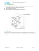
Page 13
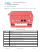
2 EQUIPMENT DESCRIPTION
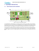
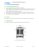
2.1 FUNCTIONAL BLOCK DIAGRAM
LNA
ADC
ADC
FPGA
DAC
DAC
LNA
AMP
PA
LNA
ADC
DAC
AMP
DL_1
DL_2
AMP
DPA_1
DPA_2
UL
DL
AC INPUT
BATT INPUT
PSU
Transceiver Transceiver
50dB
INPUT=-57dBm
-7dB47dB
OUTPUT=33dBm
53dB
INPUT = -63dBm
-7dB
44dB
OUTPUT = 27dBm
DT
MT
UL
DL
Figure 2: PS BDA Functional Block Diagram
In the downlink path, the BTS signals are received by the donor antenna of the repeater. After the duplexer,
the signals are sent to the LNA module for pre-amplification and to the digital RF integrated module for digital
filtering and frequency conversion. Then the DL signals will be sent to the downlink PA to amplify power, and
filter via the duplexer. After amplification, the signals are transmitted at the MT port to the service antenna.
In the uplink path, the mobile signals are received by the service antenna. After the MT port integrated duplexer,
the signals are sent to the LNA, integrated module for digital filtering, then to the PA for power amplification
and to the duplexer. After that, the uplink signals are sent to the donor antenna for transmission back to the
BTS.