
User's Manual

5
4. Main Board Description.
The RF signal from the input connector comes through the attenuator RA1-…-RA5, PIN attenuator (D2, D3)
and attenuator RA7 -…-RA9 to the input of the amplifying stage (Q100). Amplified power passes the harmonic
filter (the 50 Ohm stripline and capacitors CF) and directional coupler and goes to the output connector.
When the voltage, coming from the output of the input detector (D1) reaches approximately 1.2V at the base of
Q1, Q3 opens and activates the power supply voltage comparator (Q4, Q5). If the power supply voltage is less
than (17.8+0.2)V, 5V appears at Zener diode D8, which serves as the source of gate bias voltage for RF
transistor Q100, as well as the reference voltage for the main voltage regulator (Q9). This regulator limits the
output voltage to the level of about 13.6V or, if the power supply voltage is less than 13.6V, provides a voltage
drop of less than 0.15V. Transistor Q6 provides about 0.4V hysteresis in the power supply voltage comparator
and keys the “G/F” alarm signal of overvoltage.
In the case of overheating, the thermal switch SW1 via D9 blocks the input power detector and keys the “G/F”
alarm signal.
The PA has a power control loop, which is controlled by switched signals, coming from the output forwarded
power detector (DD1), output reverse power detector (DR1) and the sensor of RF transistor DC current (R13,
U1). Operational amplifiers U2-A, U2-C and diodes D20, D21 form the circuitry that switches the sensed
signals and sends the biggest of them to the loop comparator (U3-B), which controls the current of PIN
attenuator (D2, D3) – the loop adjusting element. Increase of this current is followed by an attenuation
increase.
The circuit U2-B, Q14 controls the output power level and activates a “LOW PWR” alarm signal (i.e., turns off
LED “TX”), if the output power is below the rated minimum. The circuit U2-D blocks the “LOW POWER”
signal if the load VSWR exceeds 2:1. The circuit U4, Q12 actives the “VSWR” alarm signal, when the voltage
from the reverse power sensor exceeds the voltage from the forward one. None of these circuits are active in the
stand-by mode.
Operational amplifiers U3-A, U3-C, U3-D convert the outer control voltage to the reference voltage for
comparator U3-B, providing the needed level of power regulation and thermal adjustment. Transistors Q10,
Q11 form the circuit that blocks the input power detector, when the control voltage is less than 1V.
There are four potentiometers in the Main Board: RP1 sets the DC current limit; RP2 sets the output power;
RP3 sets the “TX” indication threshold; RP4 sets the quiescent current of Q100.
5. DC Connector Board Description.
Diodes D1, D2, D3 combine the circuits of local (LED DL1, DL2, DL3) and remote (via J3) PA status
monitoring. The current source (Q1, D4) provide the constant current for alarm LED DL2. Q4 shunts LED
DL1 when the output power is below the minimum level.
The fan voltage regulator (Q2, Q3, D5) does not allow the fan voltage to be over 13.5V or keeps it at about
1.1V less than the power supply voltage.
With the aid of potentiometer RP1, a customer may set the desirable output power. Diodes D6, D7, D8
neutralize the circuit, blocking the input detector, when the control voltage is less than 1V.
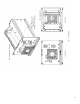
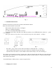
There are two jumpers (JP1, JP2) in the board – see Fig. 3. When JP1 is cut, “G/F” alarm LED at the front panel
is disconnected. When JP2 is cut, both “TX” and “VSWR” LED are disconnected.