
Service manual


57
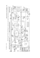
Normally IC2 would be linked directly to IC4 but, if IC3 is added, there is an option to
lower the frequency band by the use of an extra divider stage. I leave it to you to calculate
the actual
frequencies which would be achieved. Note that it might be necessary to adjust
the values of C6 and C7 if this option is used.
Construction
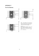
The entire unit can be built on pre-drilled copper strip board but you will never eliminate,
entirely, the interference on
receive which is caused by the fast
risetime pulses in the logic
circuit. The track layout shown can be made on single- or double-sided copper laminate and
good performance with this layout is guaranteed. The parts are readily available and should
be soldered to the board in the usual way. If a board with a copper ground plane is used,
you will have to use a drill bit to remove the copper from around all holes except those for
leads which are connected to 0 volts. As far as is practicable, these leads should be
soldered on both sides of the board.
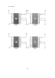
For best
decoupling performance the board should use 10nF surface mount capacitors on
the underside. These should be fitted last.
Alternatively, you might like to modify the design to suit a different radio such as the
UnidenTM or
TandyTM rigs which employ a TC9119
synthesiser chip. In this case the
10.24 MHz divider is simplified since the V.C.O. frequency is not doubled for
transmission but an additive mixing method is employed for both receive and transmit.
Consequently, only the 1.706 MHz division is required.
Pinout of the TC9119 and
information about other
synthesiser
I.C.s is available in The PLL Data Book (Ref. 3).
F
itting
a
nd s
e
tting up
Fitting the
P.C.B. to a
C.B. radio is quite straightforward. Use solder wick to de-solder
the LC7137 from the main board and fit this
I.C. into the conversion board. Remove the
10.24 MHz crystal from the radio and solder this to the conversion board. Connect the
crystal output from C5 back into the main board at the hole vacated by pin 11 of the
LC7137. The connection to pin 10 is usually not needed since its function is to ground
whatever is connected to it if a 'miscode' is presented to
inputs on pins 1 to 8. If a 'Delta
Tune' facility is present, the associated capacitors may need to be removed or they will load
the crystal unacceptably.
The
16 pin header plug should be soldered to the pads vacated by the LC7137. Make sure
that pin 1 goes to pin 1. By the way, the reason for using a
16 way ribbon is that nobody
manufactures a 20 pin header with 0.3" pitch.
Connect the
13 volt supply from the on/off switch to the board. Now, all that remains to be
done is to remove the wax from the V.C.O. coil with the aid of a tooth pick (not a soldering
iron!) and unscrew the ferrite core until the L.E.D. on the conversion board lights for both
transmit and receive. In some receivers you will need to screw the core nearly all the way
out. Tune the output coils for best performance. Do make sure that interference is within
the accepted limits. Peak the receiver coils for best reception then wax all adjusters to
prevent movement.
R
e
f
e
r
e
nc
e
s:
1) "27 - 29 MHz Conversions". Bill Sparks G8FBH and Colin Horrabin
G3SBI. "Radio
and Electronics World" November 1984 and March 1985.