
Service manual


56
By this method we blank out one V.C.O. pulse after the input square wave goes low, reset
the square wave at the end of the blanked V.C.O. pulse, then do nothing until the square
wave input goes low again. Since the circuit entirely eliminates the need for any timing
elements, but relies totally on pulse falling edges, its operation is independent of the
frequencies involved and
noods no adjustment.
Pract
i
ca
l
Cons
i
derat
i
ons
The frequencies can be as high as 19 MHz and the rise times are very short, consequently
pay careful attention to the need to decouple every I.C. with a lnF ceramic capacitor.
Connections must be as short as possible and the risk of interference to the receiver section
of the transceiver can not be stressed too highly. However, this circuit will work on pre-
drilled copper stripboard — I've done it — but better results can be obtained from a printed
circuit board with an earth plane on the component side.
The use of a low-power Schottky device for IC3 is important and IC4 must be a 74HCOO.
A 7400 is definitely not fast enough. The slightly more expensive 74ACOO works well
but, since the pulse rise times are actually shorter, more interference is generated than with
the 74HCOO and this noise affects performance during receive.
Point 'X' goes high on transmit and may be used to control a simple transistor or diode
circuit to add capacitance to the crystal oscillator whose frequency must be lowered slightly
during transmit. If this is not done,
the transmit frequency will be some 2 kHz higher than
the receive frequency. A stabilised
5 volt supply is required. I used a
78L05 regulator fed
by a 1OO Ohm resistor from the 13 volt supply, to dissipate most of the power.
Comp
l
ete
C
i
rcu
i
t
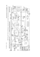
The final circuit is shown in Fig. 2 and includes a few more components to improve the
repeatability and stability of the basic design. TR3 creates a buffer between IC2 and the
10.24 MHz crystal to eliminate the effects of loading. TR1 is used to load the crystal with
an extra 8.2pF to reduce the frequency during transmit. Since 8.2pF capacitors proved hard
to obtain, I used two pairs of 15pF capacitors with each pair connected in series.
TR2 lights an L.E.D. when pin 14 of IC1 goes high to indicate that the V.C.O. is in lock:
an unnecessary frill, you might think, but it makes the re-tuning of the V.C.O. coil so
much easier. To reduce the chip count, TR5 was introduced and the gating circuit was
modified accordingly. TR4 was introduced to buffer the V.C.O. which otherwise is loaded
by IC5. Some radios tolerated the loading and some did not so this addition ensures correct
operation in any radio.
To simplify fitting the unit to a
C.B. radio, a
16 wire ribbon cable with 16 pin header at
each end was used. C15 and C16 were added to remove
interference which the ribbon
capacitance caused. Although the interference might have been eliminated by reverting to
individual wires it was considered that the simplified fitting was important and, in any case,
each constructor would connect individual wires in different ways using different lengths
which might cause interference that would be difficult to eradicate.
The unit may also be fitted to a FCC specification
radio which employs an LC7132
frequency synthesiser. This I.C. will produce frequencies which are 0.64 MHz lower, on
average, than the LC7137 since it is designed to create the old American 'FCC' band or, as
we now know it, the 'FCC' band. The channel
spacings with the LC7132 are irregular
and, for historical reasons, have 'gaps', rather than going in straightforward 10 kHz steps.