
Service manual


54
Now, the original idea was to use a simple transistor mixer to combine the V.C.O. output
with the output from IC2.
The difference frequency would then be filtered out by an L-C
'tank' circuit to be passed to the LC7137. This idea failed to work in practice and was
abandoned in
favour of the digital approach (Ref. 1) pioneered by Bill Sparks G8FBX and
Colin
Horrabin G3SBI.
Instead of mixing and filtering, we simply blank
out a certain number of Hz from the
V.C.O. output during each second. The LC7137 does not really care about the waveform
shape since it incorporates digital circuitry itself.
The occasional missing pulse, therefore, causes no problems. Since the count is less than
that produced by the V.C.O. the LC7137 increases the V.C.O. frequency until it receives
the correct average rate of pulses. The object, then, is to remove one V.C.O. pulse for
every square
wave which is produced by the 10.24 MHz divider circuit.
You might be tempted to think that simply to differentiate the square wave to form a
spike
which drives a
monostable would be a satisfactory method of generating a blanking pulse
for each leading edge of the square wave. Well, it would be, were it not for the fact that the
V.C.O. and the 10.24 MHz crystal oscillator are not
synchronised.
Also, the length of the blanking pulse needs to be varied between
transmit and receive
because the V.C.O. frequency changes. Finally, the length of the blanking pulse would
also have to be adjusted according to the channel
frequency which also alters the V.C.O.
frequency. The problem is solved by the use of two "JK
Flip-Flops" in IC3. IC3a is
programmed with J high and K low so that each time the clock input CP1 sees the falling
edge of a square wave, output Q1 goes high. This action sets J2 high. (The output of IC3b
has been reset low by the combination of R4/C3 at switch-on and is unaffected at this time
by the state of J2).
Now, thanks to the efforts of Messrs Sparks and
Horrabin who developed a way to use a
74COO as an amplifier, we have a nice, sharp V.C.O. pulse waveform appearing from
IC4b and feeding the clock input CP2. (This explanation is not difficult, just 'wordy'
;
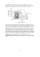
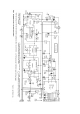
follow the circuit in Fig. 1.)
When CP2 sees the falling edge of a pulse, the contents of input K2 are transferred to /Q2
so this output goes low. IC4d is now disabled so the next V.C.O. pulse from IC4b can not
pass. IC3a input RE1 goes low and resets Q1 low so input K2 goes high. When the next
clock pulse falling edge appears from IC4b it transfers the contents of K2 to the output
which goes high, thus enabling IC4d which can then pass more clock pulses until the next
square wave falling edge hits Cp1.