
Service manual


53
APPEND
I
X
3
(not included in the original publication)
Conv
e
rt to
10
m
e
tr
e
s th
e
Chip W
a
y
You may wonder why an ordinary mortal who is not a licensed Amateur should have
wished to design a ten
metre conversion which he can't legally use. The simple answer
was, of course, money and the design was a natural development from much work on
other successful conversions for
C.B. Radios. Unfortunately, the same apathy which
prevents my learning
morse also prevented the successful marketing of the unit, so I
decided to offer the design to the world in return for a pittance.
The circuit to be described was developed for use with the most common type of
C.B.
radio which uses the ubiquitous LC7137 or LC7132 frequency
synthesiser. When the
C.B.
radio is receiving, the V.C.O. runs at the input frequency minus 10.695 MHz. On
transmit,
the V.C.O. runs at half the output frequency. For example, channel 40 normally produces a
frequency of 27.99125 MHz and to raise this to, say, 29.70 we need to add 1.70875 MHz
to the V.C.O. during receive and, during transmit, 0.853 MHz which is half that amount.
One beauty of the method to be described stems from the realisation that the 10.24 MHz
crystal oscillator output can be divided to produce almost exactly these frequencies. Mixing
the frequency with the V.C.O. output then filtering out the required sum frequency,
however, is guaranteed to create unwanted spurii at the antenna.
Bra
i
nwave
An idea came from a circuit published by Hugh Allison in "The Short Wave Magazine"
(Ref. 2) where the 10.24 MHz division frequency is subtracted from the V.C.O. output to
the P.L.L. synthesiser only. The actual V.C.O. frequency still goes directly to
the transmit
and receive circuitry. No mixing of analogue signals is necessary and transmitted
interference is thus minimised. The P.L.L. is fooled into thinking that the V.C.O.
frequency is too low and increases it accordingly!
How
It
Works
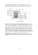
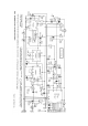
Initial tests were performed on the circuit shown in Fig. 2. IC1 is a divider
chip which is
configured to produce a divide-by-12 output on pin 12 and a divide-by-6 output on the
connection of pins 8 and 14. The 10.24 MHz reference frequency enters IC1 at pin 1.
Dividing 10.24 MHz by 12 and by 6 gives 0.853 and 1.706 MHz respectively. These
values are fractionally too low for our needs but we can adjust the 10.24 MHz reference
crystal frequency quite easily to compensate.
IC2 acts as a simple switch controlled by the TX/RX line which goes low on transmit.
During
transmit, the 0.853 MHz square wave is passed to IC3a and during receive the
1.706 MHz square wave is gated through, instead.