
Service manual


77
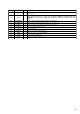
Pin No. Pin Name I/O Description
1
STKPOWER
O
Power amplifier (IC801) on/off selection signal output terminal “H”: power amplifier on
2
P O Power on/off control signal output terminal Not used (open)
3
F-RY
O
Speakers on/off relay (RY881) drive signal output terminal “H”: speakers on
4
R-RY
O
Rear speakers on/off relay drive signal output terminal “H”: speakers on Not used (open)
5 CD-POWER O
Power on/off control signal output for the CD servo section “L”: standby, “H”: power on
6 TA-MUTE O
Line muting on/off signal output terminal “L”: muting on
7
DBFB-H
O
H/L selection signal output terminal for DBFB Not used (open)
8
BYTE I
External data bus line byte selection signal input “L”: 16 bits, “H”: 8 bits
Not used (fixed at “L”)
9 CNVSS
— Ground terminal
10
SUBXIN I Sub system clock input terminal (32.768 kHz)
11
SUBXOUT O Sub system clock output terminal (32.768 kHz)
12
RESET I
System reset signal input from the reset signal generator (IC941) “L”: reset
For several hundreds msec. after the power supply rises, “L” is input, then it changes to “H”
13 XOUT
O Main system clock output terminal (16 MHz)
14 VSS
— Ground terminal
15 XIN
I Main system clock input terminal (16 MHz)
16 VCC
— Power supply terminal (+5V)
17
NMI I Non-maskable interrupt input terminal Fixed at “H” in this set
18 WAKE-UP
I System wake up signal input terminal Not used (fixed at “L”)
19 SCOR
I Subcode sync (S0+S1) detection signal input from the CXD2587Q (IC101)
20 RDS-INT I
Interrupt status input from the tuner pack Not used (open)
21 RDS-DATA I
Serial data input from the tuner pack Not used (open)
22 AC-CUT I
AC off detection signal input from the voltage detector (IC941) “L”: AC off
23 PL-CLK
O Serial data transfer clock signal output to pro-logic circuit Not used (open)
24 PL-DATA
O Serial data output to pro-logic circuit Not used (open)
25
PL-LAT O Serial data latch pulse output to pro-logic circuit Not used (open)
26 TIMER-LED
O LED drive signal output of the timer indicator Not used (open)
27
PROTECT-IN
I
Over load detection signal input for speaker output “L”: over load
28
MD-RESET O MD reset signal output terminal Not used (open)
29
IIC-SCL I/O Shift clock signal input/output terminal for the IIC bus
30
IIC-DAT I/O Data input/output terminal for the IIC bus
31
TXD — Not used (fixed at “L”)
32
SQ-DATA-IN I Subcode Q data input from the CXD2587Q (IC101)
33
SQ-CLK O Subcode Q data reading clock signal output to the CXD2587Q (IC101)
34
FL-RESET O Reset signal output to the FL driver (IC601) “L”: reset
35
FL-DATA O Serial data output to the FL driver (IC601)
36
FL-CHIP SELECT
O Chip select signal output to the FL driver (IC601) “L”: active
37
FL-CLK O Serial data transfer clock signal output to the FL driver (IC601)
38
62LAT O Serial data latch pulse signal output to the M62428AFP (IC301)
39 STBY-LED
O LED drive signal output of the standby indicator Not used (open)
40, 41
V-CINE O Not used (open)
42
FL-ON O FL power on/off control signal output terminal Not used (open)
43
POWER-ON O Standby relay drive signal output terminal “L”: standby, “H”: power on
44
B-FREQ O Not used (open)
45
FUNC-SEL1 O Function selection signal output terminal Not used (open)
• MAIN BOARD IC501 M30620MCA-A51FP (MASTER CONTROLLER)