
User manual
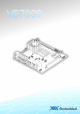

VB7009
VB7009VB7009
VB7009
User Manual
User ManualUser Manual
User Manual
viii
6.10.
Hard Disk Boot Priority.............................................................................. 63
6.11.
Advanced Chipset Features ..................................................................... 64
6.11.1.
LCD Clock Source Control ................................................................. 64
6.11.2.
LCD Backlight Control ......................................................................... 64
6.12.
PCIE Bus Control ........................................................................................ 65
6.12.1.
PCIE Root Port........................................................................................ 65
6.12.2.
PCIE Target Link Speed........................................................................ 65
6.12.3.
PCIE PE0 Control................................................................................... 65
6.12.4.
PCIE Hot-Reset Enable......................................................................... 65
6.12.5.
PCIE Root-Port-Reset Enable.............................................................. 65
6.12.6.
Maximum Payload Size........................................................................ 65
6.12.7.
PCIE ASPM Function ............................................................................. 66
6.13.
UMA & P2P Bridge Control...................................................................... 67
6.13.1.
UMA Enable ........................................................................................... 67
6.13.2.
VGA Share Memory Size ..................................................................... 67
6.13.3.
CPU Direct Access FB .......................................................................... 67
6.13.4.
Select Display Device.......................................................................... 67
6.13.5.
Select Display Device 1 ...................................................................... 67
6.13.6.
Select Display Device 2 ...................................................................... 68
6.13.7.
Panel Type .............................................................................................. 68
6.13.8.
Engine Clock Control........................................................................... 68
6.14.
CPU & PCI Bus Control ............................................................................. 69
6.14.1.
PCI Master 0 WS Write ........................................................................ 69
6.14.2.
PCI Delay Transaction .......................................................................... 69
6.14.3.
SB P2P Bridge......................................................................................... 69
6.15.
Integrated Peripherals ............................................................................... 70
6.16.
VIA OnChip IDE Device............................................................................ 71
6.16.1.
OnChip SATA ........................................................................................ 71
6.17.
VIA OnChip PCI Device ............................................................................ 72
6.17.1.
Onboard PCIE LAN............................................................................... 72
6.17.2.
Hide D1F1............................................................................................... 72
6.17.3.
OnChip HDAC Device......................................................................... 72
6.17.4.
Clear HDA Wake Enable bit .............................................................. 72